28 KiB
Voltage Amplifier PD200 - Test Bench
- Introduction
- Voltage Amplifier Requirements
- PD200 Expected characteristics
- Voltage Amplifier Model
- Noise measurement
- Transfer Function measurement
- Conclusion
Introduction
Voltage Amplifier Requirements
| Specification | |
|---|---|
| Continuous Current | > 50 [mA] |
| Output Voltage Noise (1-200Hz) | < 2 [mV rms] |
| Voltage Input Range | +/- 10 [V] |
| Voltage Output Range | -20 [V] to 150 [V] |
| Small signal bandwidth (-3dB) | > 5 [kHz] |
PD200 Expected characteristics
| Characteristics | Manual | Specification |
|---|---|---|
| Input Voltage Range | +/- 10 [V] | +/- 10 [V] |
| Output Voltage Range | -50/150 [V] | -20/150 [V] |
| Gain | 20 [V/V] | |
| Maximum RMS current | 0.9 [A] | > 50 [mA] |
| Maximum Pulse current | 10 [A] | |
| Slew Rate | 150 [V/us] | |
| Noise (10uF load) | 0.7 [mV RMS] | < 2 [mV rms] |
| Small Signal Bandwidth (10uF load) | 7.4 [kHz] | > 5 [kHz] |
| Large Signal Bandwidth (150V, 10uF) | 300 [Hz] |
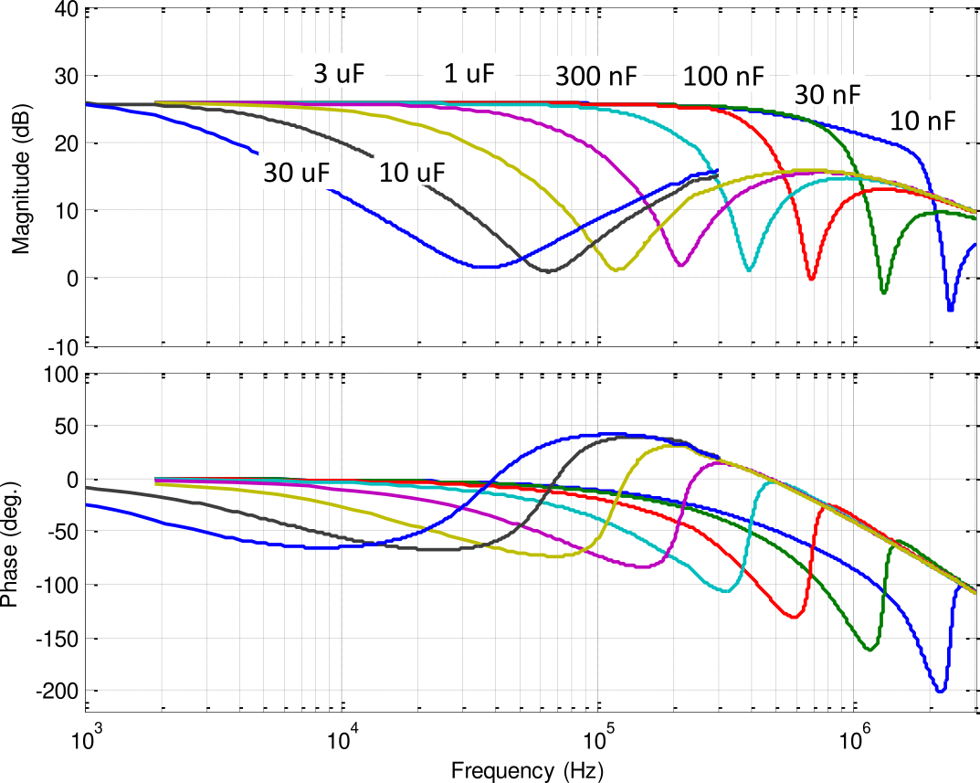
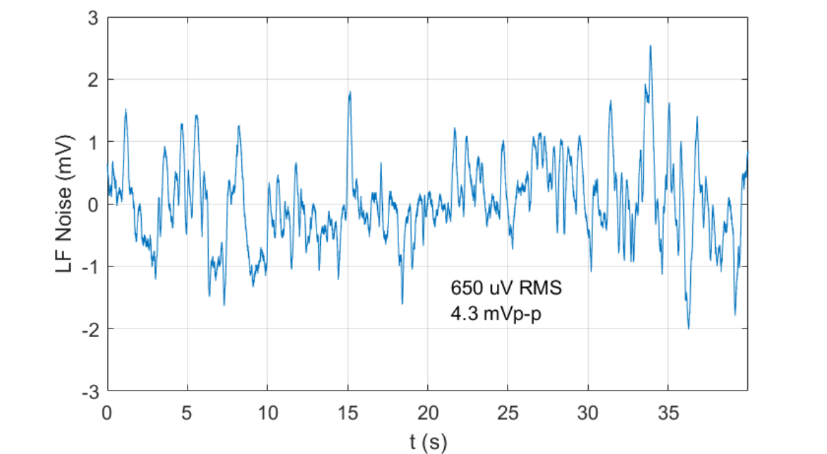
For a load capacitance of $10\,\mu F$, the expected $-3\,dB$ bandwidth is $6.4\,kHz$ (Figure fig:pd200_expected_small_signal_bandwidth) and the low frequency noise is $650\,\mu V\,\text{rms}$ (Figure fig:pd200_expected_noise).
#+caption:Expected small signal bandwidth
Voltage Amplifier Model
The Amplifier is characterized by its dynamics $G_a(s)$ from voltage inputs $V_{in}$ to voltage output $V_{out}$. Ideally, the gain from $V_{in}$ to $V_{out}$ is constant over a wide frequency band with very small phase drop.
It is also characterized by its output noise $n$. This noise is described by its Power Spectral Density.
The objective is therefore to determine the transfer function $G_a(s)$ from the input voltage to the output voltage as well as the Power Spectral Density $S_n(\omega)$ of the amplifier output noise.
As both $G_a$ and $S_n$ depends on the load capacitance, they should be measured when loading the amplifier with a $\SI{10}{\micro\farad}$ capacitor.
  \begin{tikzpicture}
    \node[block] (G) at (0,0){$G_a(s)$};
    \node[addb, right=0.8 of G] (add){};

    \draw[<-] (G.west) -- ++(-1.2, 0) node[above right]{$V_{in}$};
    \draw[->] (G.east) -- (add.west);
    \draw[->] (add.east) -- ++(1.2, 0) node[above left]{$V_{out}$};
    \draw[<-] (add.north) -- ++(0, 0.6) node[below right](n){$n$};

    \begin{scope}[on background layer]
      \node[fit={(G.south west) (n.north-|add.east)}, inner sep=8pt, draw, dashed, fill=black!20!white] (P) {};
      \node[below] at (P.north) {PD-200};
    \end{scope}
  \end{tikzpicture}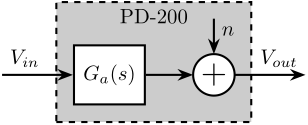
Noise measurement
Setup
Here are the documentation of the equipment used for this test bench:
- Voltage Amplifier PD200
- Load Capacitor EPCOS 10uF Multilayer Ceramic Capacitor
- Low Noise Voltage Amplifier EG&G 5113
- Speedgoat ADC IO313
The output noise of the voltage amplifier PD200 is foreseen to be around 1mV rms in a bandwidth from DC to 1MHz. If we suppose a white noise, this correspond to an amplitude spectral density:
\begin{equation} \phi_{n} \approx \frac{1\,mV}{\sqrt{1\,MHz}} = 1 \frac{\mu V}{\sqrt{Hz}} \end{equation}The RMS noise begin very small compare to the ADC resolution, we must amplify the noise before digitizing the signal. The added noise of the instrumentation amplifier should be much smaller than the noise of the PD200. We use the amplifier EG&G 5113 that has a noise of $\approx 4 nV/\sqrt{Hz}$ referred to its input which is much smaller than the noise induced by the PD200.
The gain of the low-noise amplifier can be increased until the full range of the ADC is used. This gain should be around 1000.

A low pass filter at 10kHz can be included in the EG&G amplifier in order to limit aliasing. An high pass filter at low frequency can be added if there is a problem of large offset.
Results
Pre-Amp Noise
preamp = load('mat/noise_preamp_5113.mat', 't', 'Vn', 'notes');preamp.Vn = preamp.Vn/preamp.notes.pre_amp.gain;
preamp.Vn = preamp.Vn - mean(preamp.Vn);figure;
plot(preamp.t, preamp.Vn);
xlabel('Time [s]');
ylabel('Voltage [V]');win = hanning(ceil(0.5/Ts));
[pxx, f] = pwelch(preamp.Vn, win, [], [], Fs);
preamp.pxx = pxx;
preamp.f = f;DAC (16bits) Noise
dac = load('mat/noise_preamp_5113_dac.mat', 't', 'Vn', 'notes');dac.Vn = dac.Vn/dac.notes.pre_amp.gain;dac.Vn = dac.Vn - mean(dac.Vn);figure;
plot(dac.t, 1e6*dac.Vn);
xlabel('Time [s]');
ylabel('Voltage [$\mu V$]');The PSD of the measured noise is computed and the ASD is shown in Figure fig:asd_noise_3uF.
win = hanning(ceil(0.5/Ts));

[pxx, f] = pwelch(dac.Vn, win, [], [], Fs);
dac.pxx = pxx;
dac.f = f;
SSI2V DAC (20bits) Noise
ssi2v = load('mat/noise_preamp_5113_SSI2V.mat', 't', 'Vn', 'notes');ssi2v.Vn = ssi2v.Vn/ssi2v.notes.pre_amp.gain;
ssi2v.Vn = ssi2v.Vn - mean(ssi2v.Vn);figure;
plot(ssi2v.t, 1e6*ssi2v.Vn);
xlabel('Time [s]');
ylabel('Voltage [$\mu V$]');The PSD of the measured noise is computed and the ASD is shown in Figure fig:asd_noise_3uF.
win = hanning(ceil(0.5/Ts));

[pxx, f] = pwelch(ssi2v.Vn, win, [], [], Fs);
ssi2v.pxx = pxx;
ssi2v.f = f;
Noise when shunting the input (50 Ohms) - After Warmup
The time domain measurements of the amplifier noise are shown in Figure fig:noise_shunt_time_3uF.
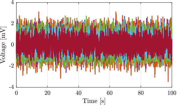
The obtained RMS and peak to peak values of the measured noises are shown in Table tab:rms_pkp_noise.
| RMS [uV] | Peak to Peak [mV] | |
|---|---|---|
| Specification [10uF] | 714.0 | 4.3 |
| PD200_1 | 565.1 | 3.7 |
| PD200_2 | 767.6 | 3.5 |
| PD200_3 | 479.9 | 3.0 |
| PD200_4 | 615.7 | 3.5 |
| PD200_5 | 651.0 | 2.4 |
| PD200_6 | 473.2 | 2.7 |
| PD200_7 | 423.1 | 2.3 |
The PSD of the measured noise is computed and the ASD is shown in Figure fig:asd_noise_3uF.
win = hanning(ceil(0.5/Ts));

for i = 1:7
    [pxx, f] = pwelch(pd200w{i}.Vn, win, [], [], Fs);
    pd200w{i}.f = f;
    pd200w{i}.pxx = pxx;
end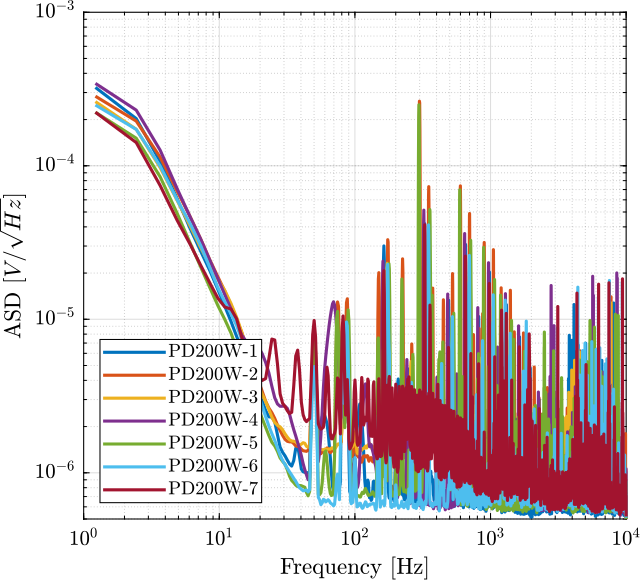
Gn = 1e-6*(s + 2*pi*40)^2/(s + 2*pi)^2;Noise with DAC at the input of the PD200
The time domain measurements of the amplifier noise are shown in Figure fig:noise_shunt_time_3uF.

The PSD of the measured noise is computed and the ASD is shown in Figure fig:asd_noise_3uF.
win = hanning(ceil(0.5/Ts));

for i = 1:7
    [pxx, f] = pwelch(pd200dac{i}.Vn, win, [], [], Fs);
    pd200dac{i}.f = f;
    pd200dac{i}.pxx = pxx;
end
The output noise of the PD200 amplifier is limited by the noise of the DAC.
TODO Noise with SSI2V at the input of the PD200
Transfer Function measurement
Setup
In order to measure the transfer function from the input voltage $V_{in}$ to the output voltage $V_{out}$, the test bench shown in Figure fig:setup-dynamics-measurement is used.
Here are the documentation of the equipment used for this test bench:
- Voltage Amplifier PD200
- Load Capacitor EPCOS 10uF Multilayer Ceramic Capacitor
- Speedgoat DAC/ADC IO313
For this measurement, the sampling frequency of the Speedgoat ADC should be as high as possible.

Maximum Frequency/Voltage to not overload the amplifier
The maximum current is 1A [rms] which corresponds to 0.7A in amplitude of the sin wave.
The impedance of the capacitance is: \[ Z_C(\omega) = \frac{1}{jC\omega} \]
Therefore the relation between the output current and the output voltage is (in amplitude): \[ V_{out} = \frac{1}{C\omega} I_{out} \]
There is a gain of 20 between the input voltage and the output voltage: \[ 20 V_{in} = \frac{1}{C\omega} I_{out} \]
For a specified voltage input amplitude $V_{in}$, the maximum frequency is then: \[ \omega_{\text{max}} = \frac{1}{20 C V_{in}} I_{out,\text{max}} \]
Iout_max = 0.7; % Maximum output current [A]
C = 3e-6; % Load Capacitance [F]

V_in = linspace(0, 5, 100); % Input Voltage [V]

w_max = 1./(20*C*V_in) * Iout_max; % [rad/s]

figure;
plot(V_in, w_max/2/pi);
xlabel('Input Voltage Amplitude [V]');
ylabel('Maximum Frequency [Hz]');
set(gca, 'yscale', 'log');
Results
First test
pd200_1V_1 = load('mat/tf_pd200_7_1V.mat', 't', 'Vin', 'Vout', 'Iout');Ts = (pd200_1V_1.t(end) - pd200_1V_1.t(1))/(length(pd200_1V_1.t)-1);
Fs = 1/Ts;win = hanning(ceil(1*Fs));
[tf_1, f] = tfestimate(pd200_1V_1.Vin, pd200_1V_1.Vout, win, [], [], 1/Ts);Conclusion
| Characteristics | Measurement | Manual | Specification |
|---|---|---|---|
| Input Voltage Range | - | +/- 10 [V] | +/- 10 [V] |
| Output Voltage Range | - | -50/150 [V] | -20/150 [V] |
| Gain | 20 [V/V] | - | |
| Maximum RMS current | 0.9 [A] | > 50 [mA] | |
| Maximum Pulse current | 10 [A] | - | |
| Slew Rate | 150 [V/us] | - | |
| Noise (10uF load) | 0.7 [mV RMS] | < 2 [mV rms] | |
| Small Signal Bandwidth (10uF load) | 7.4 [kHz] | > 5 [kHz] | |
| Large Signal Bandwidth (150V, 10uF) | 300 [Hz] | - |
