54 KiB
Voltage Amplifier PD200 - Test Bench
- Introduction
- Voltage Amplifier Requirements
- PD200 Expected characteristics
- Voltage Amplifier Model
- Noise measurement
- Transfer Function measurement
- Conclusion
This report is also available as a pdf.
Introduction
Voltage Amplifier Requirements
| Specification | |
|---|---|
| Continuous Current | > 50 [mA] |
| Output Voltage Noise (1-200Hz) | < 2 [mV rms] |
| Voltage Input Range | +/- 10 [V] |
| Voltage Output Range | -20 [V] to 150 [V] |
| Small signal bandwidth (-3dB) | > 5 [kHz] |
PD200 Expected characteristics
| Characteristics | Manual | Specification |
|---|---|---|
| Input Voltage Range | +/- 10 [V] | +/- 10 [V] |
| Output Voltage Range | -50/150 [V] | -20/150 [V] |
| Gain | 20 [V/V] | |
| Maximum RMS current | 0.9 [A] | > 50 [mA] |
| Maximum Pulse current | 10 [A] | |
| Slew Rate | 150 [V/us] | |
| Noise (10uF load) | 0.7 [mV RMS] | < 2 [mV rms] |
| Small Signal Bandwidth (10uF load) | 7.4 [kHz] | > 5 [kHz] |
| Large Signal Bandwidth (150V, 10uF) | 300 [Hz] |
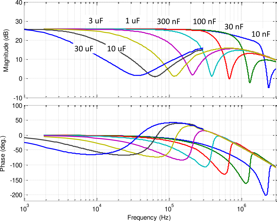
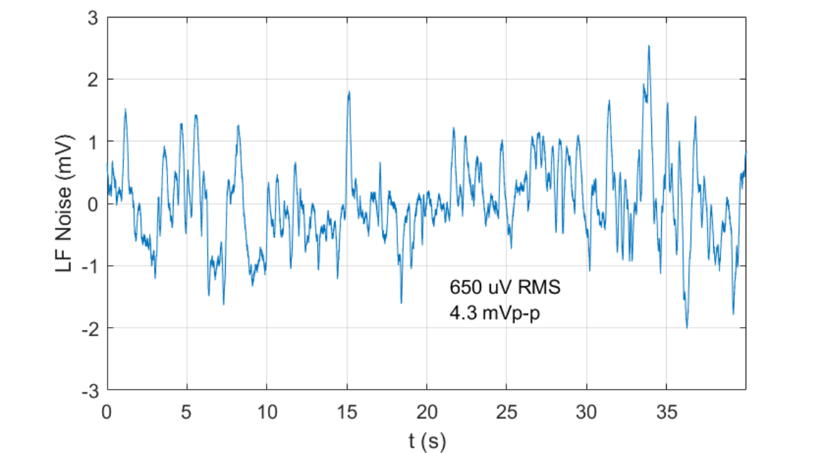
For a load capacitance of $10\,\mu F$, the expected $-3\,dB$ bandwidth is $6.4\,kHz$ (Figure fig:pd200_expected_small_signal_bandwidth) and the low frequency noise is $650\,\mu V\,\text{rms}$ (Figure fig:pd200_expected_noise).
#+caption:Expected small signal bandwidth
Voltage Amplifier Model
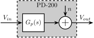
The Amplifier is characterized by its dynamics $G_p(s)$ from voltage inputs $V_{in}$ to voltage output $V_{out}$. Ideally, the gain from $V_{in}$ to $V_{out}$ is constant over a wide frequency band with very small phase drop.
It is also characterized by its output noise $n$. This noise is described by its Power Spectral Density.
The objective is therefore to determine the transfer function $G_p(s)$ from the input voltage to the output voltage as well as the Power Spectral Density $S_n(\omega)$ of the amplifier output noise.
As both $G_p$ and $S_n$ depends on the load capacitance, they should be measured when loading the amplifier with a $10\,\mu F$ capacitor.
  \begin{tikzpicture}
    \node[block] (G) at (0,0){$G_p(s)$};
    \node[addb, right=0.8 of G] (add){};

    \draw[<-] (G.west) -- ++(-1.2, 0) node[above right]{$V_{in}$};
    \draw[->] (G.east) -- (add.west);
    \draw[->] (add.east) -- ++(1.2, 0) node[above left]{$V_{out}$};
    \draw[<-] (add.north) -- ++(0, 0.6) node[below right](n){$n$};

    \begin{scope}[on background layer]
      \node[fit={(G.south west) (n.north-|add.east)}, inner sep=8pt, draw, dashed, fill=black!20!white] (P) {};
      \node[below] at (P.north) {PD-200};
    \end{scope}
\end{tikzpicture}Noise measurement
Introduction ignore
- Section sec:noise_setup
- Section sec:noise_model
- Section sec:noise_quantization
- Section sec:noise_preamp
- Section sec:noise_pd200
- Section sec:noise_dac
- Section sec:noise_full_measurement
- Section sec:noise_ssi2v
Setup
<<sec:noise_setup>>
Here are the documentation of the equipment used for this test bench:
- Voltage Amplifier PD200
- Load Capacitor EPCOS 10uF Multilayer Ceramic Capacitor
- Low Noise Voltage Amplifier EG&G 5113
- Speedgoat ADC IO313
The output noise of the voltage amplifier PD200 is foreseen to be around 1mV rms in a bandwidth from DC to 1MHz. If we suppose a white noise, this correspond to an amplitude spectral density:
\begin{equation} \phi_{n} \approx \frac{1\,mV}{\sqrt{1\,MHz}} = 1 \frac{\mu V}{\sqrt{Hz}} \end{equation}The RMS noise begin very small compare to the ADC resolution, we must amplify the noise before digitizing the signal. The added noise of the instrumentation amplifier should be much smaller than the noise of the PD200. We use the amplifier EG&G 5113 that has a noise of $\approx 4 nV/\sqrt{Hz}$ referred to its input which is much smaller than the noise induced by the PD200.
The gain of the low-noise amplifier can be increased until the full range of the ADC is used. This gain should be around 1000.
A low pass filter at 10kHz can be included in the EG&G amplifier in order to limit aliasing. An high pass filter at low frequency can be added if there is a problem of large offset.
Model of the setup
<<sec:noise_model>>
As shown in Figure fig:noise_meas_procedure, there are 4 equipment involved in the measurement:
- a Digital to Analog Convert (DAC)
- the Voltage amplifier to be measured with a gain of 20 (PD200)
- a low noise voltage amplifier with a variable gain and integrated low pass filters and high pass filters
- an Analog to Digital Converter (ADC)
Each of these equipment has some noise:
- $q_{da}$: quantization noise of the DAC
- $n_{da}$: output noise of the DAC
- $n_p$: output noise of the PD200 (what we wish to characterize)
- $n_a$: input noise of the pre amplifier
- $q_{ad}$: quantization noise of the ADC
\begin{tikzpicture}
  % DAC
  \node[DAC] (DAC) at (0,0) {DAC};
  \node[addb, right=0.4 of DAC] (addqda){};
  \node[addb, right=0.4 of addqda] (addnda){};

  % PD200
  \node[block, right=1.2 of addnda] (Gp){$G_p(s)$};
  \node[addb, right=0.4 of Gp] (addnp){};

  % Pre Amp
  \node[addb, right=1.2 of addnp] (addna){};
  \node[block, right=0.4 of addna] (Ga) {$G_a(s)$};

  % ADC
  \node[addb, right=1.2 of Ga] (addqad){};
  \node[ADC, right=0.4 of addqad] (ADC) {ADC};

  % \draw[->] (const.east) -- node[sloped]{$/$} (DAC.west);
  \draw[<-] (DAC.west) -- node[sloped]{$/$} ++(-1.0, 0);
  \draw[->] (DAC.east) -- (addqda.west);
  \draw[->] (addqda.east) -- (addnda.west);
  \draw[->] (addnda.east) -- (Gp.west);
  \draw[->] (Gp.east) -- (addnp.west);
  \draw[->] (addnp.east) -- (addna.west);
  \draw[->] (addna.east) -- (Ga.west);
  \draw[->] (Ga.east) -- (addqad.west);
  \draw[->] (addqad.east) -- (ADC.west);
  \draw[->] (ADC.east) -- node[sloped]{$/$} ++(1.0, 0) node[above left]{$n$};

  \draw[<-] (addnda.north) -- ++(0, 0.6) node[below right](nda){$n_{da}$};
  \draw[<-] (addqda.north) -- ++(0, 0.6) node[below right](qda){$q_{da}$};

  \draw[<-] (addnp.north) -- ++(0, 0.6) node[below right](np){$n_{p}$};
  \draw[<-] (addna.north) -- ++(0, 0.6) node[below right](na){$n_{a}$};

  \draw[<-] (addqad.north) -- ++(0, 0.6) node[below right](qad){$q_{ad}$};

  \coordinate[] (top) at (nda.north);
  \coordinate[] (bot) at (Ga.south);

  % DAC
  \begin{scope}[on background layer]
    \node[fit={(DAC.west|-bot) (addnda.east|-top)}, inner sep=10pt, draw, dashed, fill=black!20!white] (P) {};
    \node[above] at (P.north) {DAC};
  \end{scope}

  % PD200
  \begin{scope}[on background layer]
    \node[fit={(Gp.west|-bot) (addnp.east|-top)}, inner sep=10pt, draw, dashed, fill=black!20!white] (P) {};
    \node[above] at (P.north) {PD200};
  \end{scope}

  % 5113
  \begin{scope}[on background layer]
    \node[fit={(addna.west|-bot) (Ga.east|-top)}, inner sep=10pt, draw, dashed, fill=black!20!white] (P) {};
    \node[above] at (P.north) {Pre Amp};
  \end{scope}

  % ADC
  \begin{scope}[on background layer]
    \node[fit={(addqad.west|-bot) (ADC.east|-top)}, inner sep=10pt, draw, dashed, fill=black!20!white] (P) {};
    \node[above] at (P.north) {ADC};
  \end{scope}
\end{tikzpicture}Quantization Noise
<<sec:noise_quantization>>
The quantization noise is something that can be predicted. The Amplitude Spectral Density of the quantization noise of an ADC/DAC is equal to:
\begin{equation} \Gamma_q(\omega) = \frac{q}{\sqrt{12 f_s}} \end{equation}with:
- $q = \frac{\Delta V}{2^n}$ the quantization in [V], which is the corresponding value in [V] of the least significant bit
- $\Delta V$ is the full range of the ADC in [V]
- $n$ is the number of bits
- $f_s$ is the sample frequency in [Hz]
adc = struct();
adc.Delta_V = 20; % [V]
adc.n = 16; % number of bits
adc.Fs = 20e3; % [Hz]
adc.Gamma_q = adc.Delta_V/2^adc.n/sqrt(12*adc.Fs); % [V/sqrt(Hz)]
The obtained Amplitude Spectral Density is
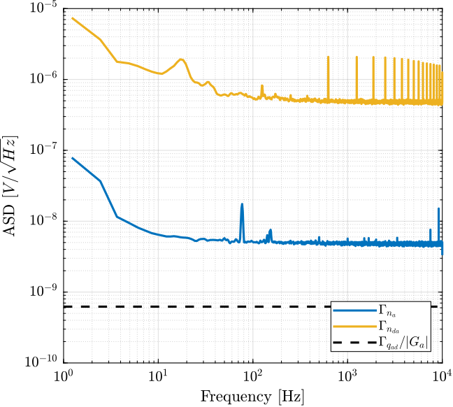
adc.Gamma_qPre Amplifier noise measurement
<<sec:noise_preamp>>
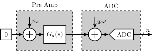
First, we wish to measure the noise of the pre-amplifier. To do so, the input of the pre-amplifier is shunted such that there is 0V at its inputs. Then, the gain of the amplifier is increase until the measured signal on the ADC is much larger than the quantization noise.
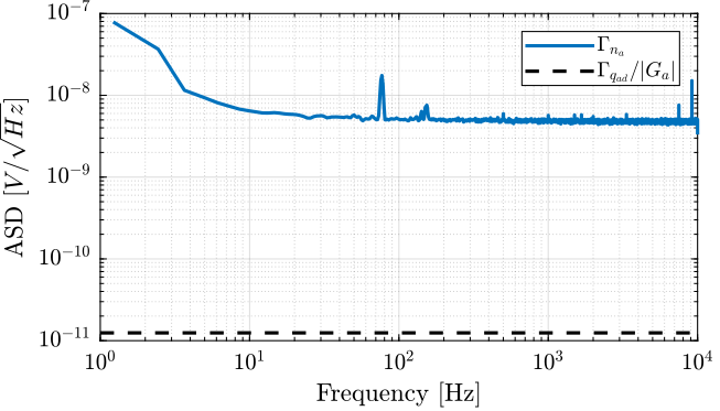
The Amplitude Spectral Density $\Gamma_n(\omega)$ of the measured signal $n$ is computed. Finally, the Amplitude Spectral Density of $n_a$ can be computed taking into account the gain of the pre-amplifier:
\begin{equation} \Gamma_{n_a}(\omega) \approx \frac{\Gamma_n(\omega)}{|G_a(\omega)|} \end{equation}This is true if the quantization noise $\Gamma_{q_{ad}}$ is negligible.
\begin{tikzpicture}
  \node[block={0.6cm}{0.6cm}] (const) {$0$};
  % Pre Amp
  \node[addb, right=0.6 of const] (addna) {};
  \node[block, right=0.4 of addna] (Ga) {$G_a(s)$};

  % ADC
  \node[addb, right=1.2 of Ga] (addqad){};
  \node[ADC, right=0.4 of addqad] (ADC) {ADC};

  \draw[->] (const.east) -- (addna.west);
  \draw[->] (addna.east) -- (Ga.west);
  \draw[->] (Ga.east) -- (addqad.west);
  \draw[->] (addqad.east) -- (ADC.west);
  \draw[->] (ADC.east) -- node[sloped]{$/$} ++(1.0, 0) node[above left]{$n$};

  \draw[<-] (addna.north) -- ++(0, 0.6) node[below right](na){$n_{a}$};
  \draw[<-] (addqad.north) -- ++(0, 0.6) node[below right](qad){$q_{ad}$};

  \coordinate[] (top) at (na.north);
  \coordinate[] (bot) at (Ga.south);

  % 5113
  \begin{scope}[on background layer]
    \node[fit={(addna.west|-bot) (Ga.east|-top)}, inner sep=10pt, draw, dashed, fill=black!20!white] (P) {};
    \node[above] at (P.north) {Pre Amp};
  \end{scope}

  % ADC
  \begin{scope}[on background layer]
    \node[fit={(addqad.west|-bot) (ADC.east|-top)}, inner sep=10pt, draw, dashed, fill=black!20!white] (P) {};
    \node[above] at (P.north) {ADC};
  \end{scope}
\end{tikzpicture}The gain of the low noise amplifier is set to
ans = preamp.notes.pre_amp.gain% Hanning window
win = hanning(ceil(0.5/Ts));
% Power Spectral Density
[pxx, f] = pwelch(preamp.Vn, win, [], [], Fs);
% Save the results inside the struct
preamp.pxx = pxx;
preamp.f = f;The obtained Amplitude Spectral Density of the Low Noise Voltage Amplifier is shown in Figure fig:asd_preamp. The obtained noise amplitude is very closed to the one specified in the documentation of $4nV/\sqrt{Hz}$ at 1kHZ.
PD200 noise measurement
<<sec:noise_pd200>>
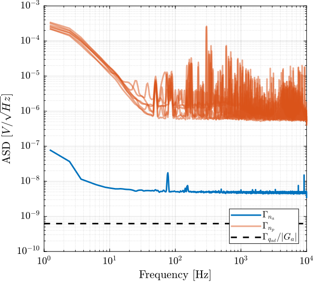
The input of the PD200 amplifier is shunted such that there is 0V between its inputs. Then the gain of the pre-amplifier is increased in order to measure a signal much larger than the quantization noise of the ADC. We compute the Amplitude Spectral Density of the measured signal $\Gamma_n(\omega)$. The Amplitude Spectral Density of $n_p$ can be computed taking into account the gain of the pre-amplifier:
\begin{equation} \Gamma_{n_p}(\omega) = \frac{\Gamma_n(\omega)}{|G_a(\omega)|} \end{equation}And we verify that this is indeed the noise of the PD200 and not the noise of the pre-amplifier by checking that:
\begin{equation} \Gamma_{n_p} \ll \Gamma_{n_a} \end{equation}\begin{tikzpicture}
\node[block={0.6cm}{0.6cm}] (const) {$0$};
% PD200
\node[block, right=0.6 of const] (Gp){$G_p(s)$};
\node[addb, right=0.4 of Gp] (addnp){};
% Pre Amp
\node[addb, right=1.2 of addnp] (addna) {};
\node[block, right=0.4 of addna] (Ga) {$G_a(s)$};
% ADC
\node[addb, right=1.2 of Ga] (addqad){};
\node[ADC, right=0.4 of addqad] (ADC) {ADC};
\draw[->] (const.east) -- (Gp.west);
\draw[->] (Gp.east) -- (addnp.west);
\draw[->] (addnp.east) -- (addna.west);
\draw[->] (addna.east) -- (Ga.west);
\draw[->] (Ga.east) -- (addqad.west);
\draw[->] (addqad.east) -- (ADC.west);
\draw[->] (ADC.east) -- node[sloped]{$/$} ++(1.0, 0) node[above left]{$n$};
\draw[<-] (addnp.north) -- ++(0, 0.6) node[below right](np){$n_{p}$};
\draw[<-] (addna.north) -- ++(0, 0.6) node[below right](na){$n_{a}$};
\draw[<-] (addqad.north) -- ++(0, 0.6) node[below right](qad){$q_{ad}$};
\coordinate[] (top) at (na.north);
\coordinate[] (bot) at (Ga.south);
% PD200
\begin{scope}[on background layer]
\node[fit={(Gp.west|-bot) (addnp.east|-top)}, inner sep=10pt, draw, dashed, fill=black!20!white] (P) {};
\node[above] at (P.north) {PD200};
\end{scope}
% 5113
\begin{scope}[on background layer]
\node[fit={(addna.west|-bot) (Ga.east|-top)}, inner sep=10pt, draw, dashed, fill=black!20!white] (P) {};
\node[above] at (P.north) {Pre Amp};
\end{scope}
% ADC
\begin{scope}[on background layer]
\node[fit={(addqad.west|-bot) (ADC.east|-top)}, inner sep=10pt, draw, dashed, fill=black!20!white] (P) {};
\node[above] at (P.north) {ADC};
\end{scope}
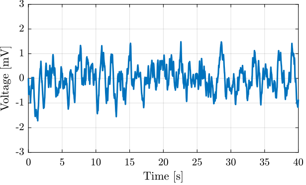
\end{tikzpicture}The measured low frequency noise $n_p$ of one of the amplifiers is shown in Figure fig:pd200_noise_time_lpf. It is very similar to the one specified in the datasheet in Figure fig:pd200_expected_noise.
The obtained RMS and peak to peak values of the measured noises are shown in Table tab:rms_pkp_noise.
| RMS [uV] | Peak to Peak [mV] | |
|---|---|---|
| Specification [10uF] | 714.0 | 4.3 |
| PD200_1 | 565.1 | 3.7 |
| PD200_2 | 767.6 | 3.5 |
| PD200_3 | 479.9 | 3.0 |
| PD200_4 | 615.7 | 3.5 |
| PD200_5 | 651.0 | 2.4 |
| PD200_6 | 473.2 | 2.7 |
| PD200_7 | 423.1 | 2.3 |
The Amplitude Spectral Density of the measured noise is now computed and shown in Figure fig:asd_noise_3uF_warmup.
DAC noise measurement
<<sec:noise_dac>>
In order not to have any quantization noise, we impose the DAC to output a zero voltage. The gain of the low noise amplifier is adjusted to
The Amplitude Spectral Density $\Gamma_n(\omega)$ of the measured signal is computed. The Amplitude Spectral Density of $n_{da}$ can be computed taking into account the gain of the pre-amplifier:
\begin{equation} \Gamma_{n_{da}}(\omega) = \frac{\Gamma_m(\omega)}{|G_a(\omega)|} \end{equation}And it is verify that the Amplitude Spectral Density of $n_{da}$ is much larger than the one of $n_a$:
\begin{equation} \Gamma_{n_{da}} \gg \Gamma_{n_a} \end{equation}\begin{tikzpicture}
\node[block={0.6cm}{0.6cm}] (const) {$0$};
% DAC
\node[DAC, right=0.6 of const] (DAC) {DAC};
\node[addb, right=0.4 of DAC] (addnda){};
% Pre Amp
\node[addb, right=1.2 of addnda] (addna) {};
\node[block, right=0.4 of addna] (Ga) {$G_a(s)$};
% ADC
\node[addb, right=1.2 of Ga] (addqad){};
\node[ADC, right=0.4 of addqad] (ADC) {ADC};
\draw[->] (const.east) -- node[sloped]{$/$} (DAC.west);
\draw[->] (DAC.east) -- (addnda.west);
\draw[->] (addnda.east) -- (addna.west);
\draw[->] (addna.east) -- (Ga.west);
\draw[->] (Ga.east) -- (addqad.west);
\draw[->] (addqad.east) -- (ADC.west);
\draw[->] (ADC.east) -- node[sloped]{$/$} ++(1.0, 0);
\draw[<-] (addnda.north) -- ++(0, 0.6) node[below right](nda){$n_{da}$};
\draw[<-] (addna.north) -- ++(0, 0.6) node[below right](na){$n_{a}$};
\draw[<-] (addqad.north) -- ++(0, 0.6) node[below right](qad){$q_{ad}$};
\coordinate[] (top) at (na.north);
\coordinate[] (bot) at (Ga.south);
% DAC
\begin{scope}[on background layer]
\node[fit={(DAC.west|-bot) (addnda.east|-top)}, inner sep=10pt, draw, dashed, fill=black!20!white] (P) {};
\node[above] at (P.north) {DAC};
\end{scope}
% 5113
\begin{scope}[on background layer]
\node[fit={(addna.west|-bot) (Ga.east|-top)}, inner sep=10pt, draw, dashed, fill=black!20!white] (P) {};
\node[above] at (P.north) {Pre Amp};
\end{scope}
% ADC
\begin{scope}[on background layer]
\node[fit={(addqad.west|-bot) (ADC.east|-top)}, inner sep=10pt, draw, dashed, fill=black!20!white] (P) {};
\node[above] at (P.north) {ADC};
\end{scope}
\end{tikzpicture}Total noise measurement
<<sec:noise_full_measurement>>
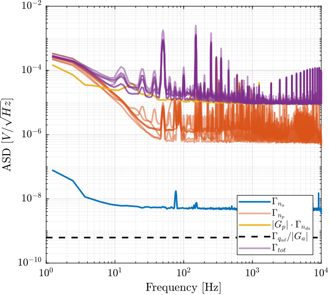
Let's now analyze the measurement of the setup in Figure fig:noise_meas_procedure.
The PSD of the measured noise is computed and the ASD is shown in Figure fig:asd_noise_tot.
win = hanning(ceil(0.5/Ts));

for i = 1:7
    [pxx, f] = pwelch(pd200dac{i}.Vn, win, [], [], Fs);
    pd200dac{i}.f = f;
    pd200dac{i}.pxx = pxx;
endThe output noise of the PD200 amplifier is limited by the noise of the DAC. Having a DAC with lower noise could lower the output noise of the PD200. SSI2V DACs will be used to verify that.
20bits DAC noise measurement
<<sec:noise_ssi2v>> Let's now measure the noise of another DAC called the "SSI2V" (doc). It is a 20bits DAC with an output of +/-10.48 V and a very low noise.
The measurement setup is the same as the one in Figure fig:noise_measure_setup_dac.
win = hanning(ceil(0.5/Ts));

[pxx, f] = pwelch(ssi2v.Vn, win, [], [], Fs);
ssi2v.pxx = pxx;
ssi2v.f = f;
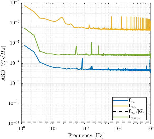
The obtained noise of the SSI2V DAC is shown in Figure fig:asd_ssi2v_noise and compared with the noise of the 16bits DAC. It is shown to be much smaller (~1 order of magnitude).
Using the SSI2V as the DAC with the PD200 should give much better noise output than using the 16bits DAC. The limiting factor should then be the noise of the PD200 itself.
Transfer Function measurement
Setup
In order to measure the transfer function from the input voltage $V_{in}$ to the output voltage $V_{out}$, the test bench shown in Figure fig:setup-dynamics-measurement is used.
Here are the documentation of the equipment used for this test bench:
- Voltage Amplifier PD200
- Load Capacitor EPCOS 10uF Multilayer Ceramic Capacitor
- Speedgoat DAC/ADC IO313
For this measurement, the sampling frequency of the Speedgoat ADC should be as high as possible.

Maximum Frequency/Voltage to not overload the amplifier
The maximum current is 1A [rms] which corresponds to 0.7A in amplitude of the sin wave.
The impedance of the capacitance is: \[ Z_C(\omega) = \frac{1}{jC\omega} \]
Therefore the relation between the output current amplitude and the output voltage amplitude for sinusoidal waves of frequency $\omega$: \[ V_{out} = \frac{1}{C\omega} I_{out} \]
Moreover, there is a gain of 20 between the input voltage and the output voltage: \[ 20 V_{in} = \frac{1}{C\omega} I_{out} \]
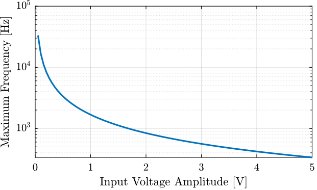
For a specified voltage input amplitude $V_{in}$, the maximum frequency at which the output current reaches its maximum value is: \[ \omega_{\text{max}} = \frac{1}{20 C V_{in}} I_{out,\text{max}} \]
$\omega_max$ as a function of $V_{in}$ is shown in Figure fig:max_frequency_voltage.
Obtained Transfer Functions
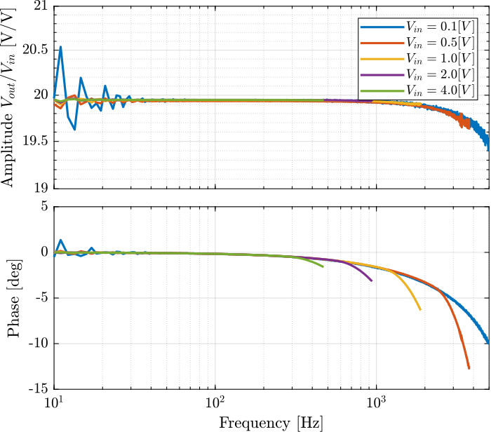
Several identifications using sweep sin were performed with input voltage amplitude ranging from 0.1V to 4V.
The obtained frequency response functions are shown in Figure fig:pd200_tf_voltage. As the input voltage increases, the voltage drop is increasing.
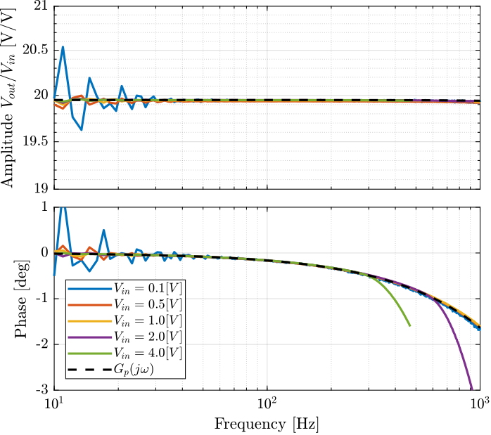
The small signal transfer function of the amplifier can be approximated by a first order low pass filter.
Gp = 19.95/(1 + s/2/pi/35e3);The comparison from the model and measurements are shown in Figure fig:tf_pd200_model.
Conclusion
| Characteristics | Measurement | Manual | Specification |
|---|---|---|---|
| Input Voltage Range | - | +/- 10 [V] | +/- 10 [V] |
| Output Voltage Range | - | -50/150 [V] | -20/150 [V] |
| Gain | 20 [V/V] | - | |
| Maximum RMS current | 0.9 [A] | > 50 [mA] | |
| Maximum Pulse current | 10 [A] | - | |
| Slew Rate | 150 [V/us] | - | |
| Noise (10uF load) | 0.7 [mV RMS] | < 2 [mV rms] | |
| Small Signal Bandwidth (10uF load) | 7.4 [kHz] | > 5 [kHz] | |
| Large Signal Bandwidth (150V, 10uF) | 300 [Hz] | - |
