100 KiB
Nano Active Stabilization System - Instrumentation
- Introduction
- Dynamic Error Budgeting
- Choice of Instrumentation
- Characterization of Instrumentation
- Conclusion
- Bibliography
- Footnotes
Introduction ignore
This chapter presents an approach to selecting and validating appropriate instrumentation for the Nano Active Stabilization System (NASS), ensuring each component meets specific performance requirements. Figure ref:fig:detail_instrumentation_plant illustrates the control diagram with all relevant noise sources whose effects on sample position will be evaluated throughout this analysis.
The selection process follows a three-stage methodology. First, dynamic error budgeting is performed in Section ref:sec:detail_instrumentation_dynamic_error_budgeting to establish maximum acceptable noise specifications for each instrumentation component (ADC, DAC, and voltage amplifier). This analysis utilizes the multi-body model with a 2DoF APA model, focusing particularly on the vertical direction due to its more stringent requirements. From the calculated transfer functions, maximum acceptable amplitude spectral densities for each noise source are derived.
Section ref:sec:detail_instrumentation_choice then presents the selection of appropriate components based on these noise specifications and additional requirements.
Finally, Section ref:sec:detail_instrumentation_characterization validates the selected components through experimental testing. Each instrument is characterized individually, measuring actual noise levels and performance characteristics. The measured noise characteristics are then incorporated into the multi-body model to confirm that the combined effect of all instrumentation noise sources remains within acceptable limits.
\begin{tikzpicture}
  % Blocs
  \node[block={2.0cm}{2.0cm}, align=center] (plant) {NASS};

  \coordinate[] (inputVa)  at ($(plant.south west)!0.5!(plant.north west)$);
  \coordinate[] (outputVs) at ($(plant.south east)!0.7!(plant.north east)$);
  \coordinate[] (outputde) at ($(plant.south east)!0.3!(plant.north east)$);

  \node[addb={+}{}{}{}{}, left=0.8 of inputVa] (ampl_noise) {};
  \node[block={1.0cm}{1.0cm}, left=0.4 of ampl_noise] (ampl_tf) {$G_{\text{ampl}}$};

  \node[addb={+}{}{}{}{}, left=0.8 of ampl_tf] (dac_noise) {};
  \node[DAC, left=0.4 of dac_noise] (dac_tf) {};

  \node[addb={+}{}{}{}{}, left=1.0 of dac_tf] (iff_sum) {};

  \node[block={1.0cm}{1.0cm}, above=0.4 of iff_sum] (Kiff) {$\bm{K}_{\text{IFF}}$};
  \node[block={1.0cm}{1.0cm}, left=0.4 of iff_sum] (Khac) {$\bm{K}_{\text{HAC}}$};

  \node[addb={+}{}{}{}{}, right=0.8 of outputVs] (adc_noise) {};
  \node[ADC, right=0.4 of adc_noise] (adc_tf) {};

  \draw[->] (iff_sum.east)    --node[midway, above]{$\bm{u}$} node[near start, sloped]{$/$} (dac_tf.west);
  \draw[->] (dac_tf.east)     -- (dac_noise.west);
  \draw[->] (dac_noise.east)  -- (ampl_tf.west);
  \draw[->] (ampl_tf.east)    -- (ampl_noise.west);
  \draw[->] (ampl_noise.east)    -- (inputVa)node[above left]{$\bm{V}_a$};
  \draw[->] (outputVs)node[above right]{$\bm{V}_s$} -- (adc_noise.west);
  \draw[->] (adc_noise.east)     -- (adc_tf.west);
  \draw[->] (adc_tf.east)  -| ++(0.4, 1.8) -| node[near start, sloped]{$/$} (Kiff.north);
  \draw[->] (Kiff.south)       -- node[sloped]{$/$} (iff_sum.north);
  \draw[->] (outputde)node[above right]{$\bm{\epsilon}_{\mathcal{L}}$} -| ++(0.6, -1.0) -| node[near start, sloped]{$/$} ($(Khac.west)+(-0.6, 0)$) -- (Khac.west);
  \draw[->] (Khac.east)       -- node[sloped]{$/$} (iff_sum.west);

  \draw[<-] (dac_noise.north)  -- ++(0, 0.8)coordinate(dac_noise_input)  node[below left]{$n_{\text{da}}$};
  \draw[<-] (ampl_noise.north) -- ++(0, 0.8)coordinate(ampl_noise_input) node[below left]{$n_{\text{amp}}$};
  \draw[<-] (adc_noise.north)  -- ++(0, 0.8)coordinate(adc_noise_input)  node[below right]{$n_{\text{ad}}$};

  \begin{scope}[on background layer]
    \node[fit={(dac_tf.south west) (dac_noise.east|-dac_noise_input)}, fill=colorblue!20!white, draw, dashed, inner sep=4pt] (dac_system) {};
    \node[anchor={north}] at (dac_system.south){$\text{DAC}$};
  \end{scope}

  \begin{scope}[on background layer]
    \node[fit={(ampl_tf.south west) (ampl_noise.east|-ampl_noise_input)}, fill=colorred!20!white, draw, dashed, inner sep=4pt] (ampl_system) {};
    \node[anchor={north}] at (ampl_system.south){$\text{Amplifier}$};
  \end{scope}

  \begin{scope}[on background layer]
    \node[fit={(adc_noise.south -| adc_noise.west) (adc_tf.east|-adc_noise_input)}, fill=coloryellow!20!white, draw, dashed, inner sep=4pt] (adc_system) {};
    \node[anchor={north}] at (adc_system.south){$\text{ADC}$};
  \end{scope}

  \begin{scope}[on background layer]
    \node[fit={(Khac.south west) (Kiff.north east)}, fill=black!20!white, draw, dashed, inner sep=4pt] (control_system) {};
    \node[anchor={north}] at (control_system.south){$\text{RT Controller}$};
  \end{scope}
\end{tikzpicture}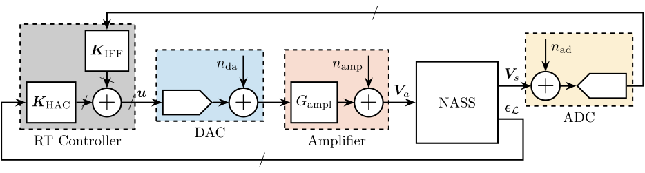
Dynamic Error Budgeting
<<sec:detail_instrumentation_dynamic_error_budgeting>>
Introduction ignore
The primary goal of this analysis is to establish specifications for the maximum allowable noise levels of the instrumentation used for the NASS (ADC, DAC, and voltage amplifier) that would result in acceptable vibration levels in the system.
The procedure involves determining the closed-loop transfer functions from various noise sources to positioning error (Section ref:ssec:detail_instrumentation_cl_sensitivity). This analysis is conducted using the multi-body model with a 2-DoF Amplified Piezoelectric Actuator model that incorporates voltage inputs and outputs. Only the vertical direction is considered in this analysis as it presents the most stringent requirements; the horizontal directions are subject to less demanding constraints.
From these transfer functions, the maximum acceptable Amplitude Spectral Density (ASD) of the noise sources is derived (Section ref:ssec:detail_instrumentation_max_noise_specs). Since the voltage amplifier gain affects the amplification of DAC noise, an assumption of an amplifier gain of 20 was made.
Closed-Loop Sensitivity to Instrumentation Disturbances
<<ssec:detail_instrumentation_cl_sensitivity>>
Several key noise sources are considered in the analysis (Figure ref:fig:detail_instrumentation_plant). These include the output voltage noise of the DAC ($n_{da}$), the output voltage noise of the voltage amplifier ($n_{amp}$), and the voltage noise of the ADC measuring the force sensor stacks ($n_{ad}$).
Encoder noise, which is only used to estimate $R_z$, has been found to have minimal impact on the vertical sample error and is therefore omitted from this analysis for clarity.
The transfer functions from these three noise sources (for one strut) to the vertical error of the sample are estimated from the multi-body model, which includes the APA300ML and the designed flexible joints (Figure ref:fig:detail_instrumentation_noise_sensitivities).
%% Identify the transfer functions from disturbance sources to vertical position error
% Let's initialize all the stages with default parameters.
initializeGround();
initializeGranite();
initializeTy();
initializeRy();
initializeRz();
initializeMicroHexapod();
initializeSample('m', 1);
initializeSimplifiedNanoHexapod();

initializeSimscapeConfiguration();
initializeDisturbances('enable', false);
initializeLoggingConfiguration('log', 'none');
initializeController('type', 'hac-iff');
initializeReferences();

% Decentralized IFF controller
wz = 2*pi*2;
xiz = 0.7;
Ghpf = (s^2/wz^2)/(s^2/wz^2 + 2*xiz*s/wz + 1);

Kiff = -200 * ...              % Gain
       1/(0.01*2*pi + s) * ... % LPF: provides integral action
       Ghpf * ...              % 2nd order HPF (limit low frequency gain)
       eye(6);                 % Diagonal 6x6 controller (i.e. decentralized)

% Centralized HAC
wc = 2*pi*10; % Wanted crossover [rad/s]
H_int = wc/s; % Integrator
a  = 2;  % Amount of phase lead / width of the phase lead / high frequency gain
H_lead = 1/sqrt(a)*(1 + s/(wc/sqrt(a)))/(1 + s/(wc*sqrt(a))); % Lead to increase phase margin
H_lpf = 1/(1 + s/2/pi/80); % Low Pass filter to increase robustness

Khac = -5e4    * ... % Gain
        H_int  * ... % Integrator
        H_lead * ... % Low Pass filter
        H_lpf  * ... % Low Pass filter
        eye(6);      % 6x6 Diagonal

% Input/Output definition
clear io; io_i = 1;
io(io_i) = linio([mdl, '/dac_noise'],      1, 'input'); io_i = io_i + 1; % DAC noise [V]
io(io_i) = linio([mdl, '/amp_noise'],      1, 'input'); io_i = io_i + 1; % Voltage Amplifier noise [V]
io(io_i) = linio([mdl, '/NASS/adc_noise'], 1, 'input'); io_i = io_i + 1; % ADC noise [V]
io(io_i) = linio([mdl, '/NASS/enc_noise'], 1, 'input'); io_i = io_i + 1; % Encoder noise [m]
io(io_i) = linio([mdl, '/NASS'],           2, 'output', [], 'z');  io_i = io_i + 1; % Vertical error [m]
io(io_i) = linio([mdl, '/NASS'],           2, 'output', [], 'y');  io_i = io_i + 1; % Lateral error [m]

Gd = linearize(mdl, io);
Gd.InputName  = {...
    'nda1',  'nda2',  'nda3',  'nda4',  'nda5',  'nda6',  ... % DAC and Voltage amplifier noise
    'namp1',  'namp2',  'namp3',  'namp4',  'namp5',  'namp6',  ... % DAC and Voltage amplifier noise
    'nad1', 'nad2', 'nad3', 'nad4', 'nad5', 'nad6', ... % ADC noise
    'ddL1', 'ddL2', 'ddL3', 'ddL4', 'ddL5', 'ddL6'  ... % Encoder noise
};
Gd.OutputName = {'y', 'z'}; % Vertical error of the sample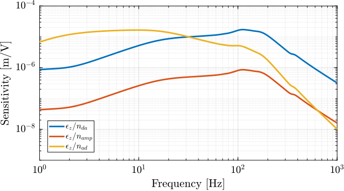
Estimation of maximum instrumentation noise
<<ssec:detail_instrumentation_max_noise_specs>>
The most stringent requirement for the system is maintaining vertical vibrations below the smallest expected beam size of $100\,\text{nm}$, which corresponds to a maximum allowed vibration of $15\,\text{nm RMS}$.
Several assumptions regarding the noise characteristics have been made. The DAC, ADC, and amplifier noise are considered uncorrelated, which is a reasonable assumption. Similarly, the noise sources corresponding to each strut are also assumed to be uncorrelated. This means that the power spectral densities (PSD) of the different noise sources are summed.
The system symmetry has been utilized to further simplify the analysis. The effect of all struts on the vertical errors is identical, as verified from the extracted sensitivity curves. Therefore, only one strut is considered for this analysis, and the total effect of the six struts is calculated as six times the effect of one strut in terms of power, which translates to a factor of $\sqrt{6} \approx 2.5$ for RMS values.
In order to derive specifications in terms of noise spectral density for each instrumentation component, a white noise profile is assumed, which is typical for these components.
The noise specification is computed such that if all components operate at their maximum allowable noise levels, the specification for vertical error will still be met. While this represents a pessimistic approach, it provides a reasonable estimate of the required specifications.
Based on this analysis, the obtained maximum noise levels are as follows: DAC maximum output noise ASD is established at $14\,\mu V/\sqrt{\text{Hz}}$, voltage amplifier maximum output voltage noise ASD at $280\,\mu V/\sqrt{\text{Hz}}$, and ADC maximum measurement noise ASD at $11\,\mu V/\sqrt{\text{Hz}}$. In terms of RMS noise, these translate to less than $1\,\text{mV RMS}$ for the DAC, less than $20\,\text{mV RMS}$ for the voltage amplifier, and less than $0.8\,\text{mV RMS}$ for the ADC.
If the Amplitude Spectral Density of the noise of the ADC, DAC, and voltage amplifiers all remain below these specified maximum levels, then the induced vertical error will be maintained below 15nm RMS.
% Maximum wanted effect of each noise source on the vertical error
% Specifications: 15nm RMS
% divide by sqrt(6) because 6 struts
% divide by sqrt(3) because 3 considered noise sources
max_asd_z = 15e-9 / sqrt(6) / sqrt(3); % [m/sqrt(Hz)]

% Suppose unitary flat noise ASD => compute the effect on vertical noise
unit_asd = ones(1, length(freqs));
rms_unit_asd_dac = sqrt(sum((unit_asd.*abs(squeeze(freqresp(Gd('z', 'nda1' ), freqs, 'Hz'))).').^2));
rms_unit_asd_amp = sqrt(sum((unit_asd.*abs(squeeze(freqresp(Gd('z', 'namp1'), freqs, 'Hz'))).').^2));
rms_unit_asd_adc = sqrt(sum((unit_asd.*abs(squeeze(freqresp(Gd('z', 'nad1' ), freqs, 'Hz'))).').^2));

% Obtained maximum ASD for different instruments
max_dac_asd = max_asd_z./rms_unit_asd_dac; % [V/sqrt(Hz)]
max_amp_asd = max_asd_z./rms_unit_asd_amp; % [V/sqrt(Hz)]
max_adc_asd = max_asd_z./rms_unit_asd_adc; % [V/sqrt(Hz)]

% Estimation of the equivalent RMS noise
max_dac_rms = 1e3*max_dac_asd*sqrt(5e3) % [mV RMS]
max_amp_rms = 1e3*max_amp_asd*sqrt(5e3) % [mV RMS]
max_adc_rms = 1e3*max_adc_asd*sqrt(5e3) % [mV RMS]
Choice of Instrumentation
<<sec:detail_instrumentation_choice>>
Introduction ignore
The selection of appropriate instrumentation components was based on the noise specifications derived in Section ref:sec:detail_instrumentation_dynamic_error_budgeting and other relevant specifications that will be further developed.
This section presents the evaluation process for ADCs, DACs, voltage amplifiers, and relative positioning sensors, detailing the comparison between different options and justifying the final selections.
Piezoelectric Voltage Amplifier
Introduction ignore
Several characteristics of piezoelectric voltage amplifiers must be considered for this application. To utilize the full stroke of the piezoelectric actuator, the voltage output should range between $-20$ and $150\,V$. The amplifier should accept an analog input voltage, preferably in the range of $-10$ to $10\,V$, as this is standard for most DACs.
Small signal Bandwidth and Output Impedance
Small signal bandwidth is particularly important for feedback applications as it can limit the overall bandwidth of the complete feedback system.
A simplified electrical model of a voltage amplifier connected to a piezoelectric stack is shown in Figure ref:fig:detail_instrumentation_amp_output_impedance. This model is valid for small signals and provides insight into the small signal bandwidth limitation cite:&fleming14_desig_model_contr_nanop_system, chap. 14. In this model, $R_o$ represents the output impedance of the amplifier. When combined with the piezoelectric load (represented as a capacitance $C_p$), it forms a first order low pass filter described by eqref:eq:detail_instrumentation_amp_output_impedance.
\begin{equation}\label{eq:detail_instrumentation_amp_output_impedance} \frac{V_a}{V_i}(s) = \frac{1}{1 + \frac{s}{ω_0}}, \quad ω_0 = \frac{1}{R_o C_p}
\end{equation}
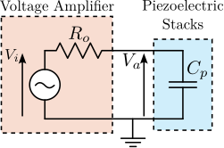
Consequently, the small signal bandwidth depends on the load capacitance and decreases as the load capacitance increases. For the APA300ML, the capacitive load of the two piezoelectric stacks corresponds to $C_p = 8.8\,\mu F$. If a small signal bandwidth of $f_0 = \frac{\omega_0}{2\pi} = 5\,\text{kHz}$ is desired, the voltage amplifier output impedance should be less than $R_0 = 3.6\,\Omega$.
Cp = 8.8e-6; % Capacitive load of the two piezoelectric actuators
f0 = 5e3; % Wanted low signal bandwidth [Hz]
Ro_max = 1/(2*pi*f0 * Cp); % Maximum wanted output impedance [Ohm]
Large signal Bandwidth
Large signal bandwidth relates to the maximum output capabilities of the amplifier in terms of amplitude as a function of frequency.
Since the primary function of the NASS is position stabilization rather than scanning, this specification is less critical than the small signal bandwidth. However, considering potential scanning capabilities, a worst-case scenario of a constant velocity scan (triangular reference signal) with a repetition rate of $f_r = 100\,\text{Hz}$ using the full voltage range of the piezoelectric actuator ($V_{pp} = 170\,V$) is considered.
There are two limiting factors for large signal bandwidth that should be evaluated:
- Slew rate, which should exceed $2 \cdot V_{pp} \cdot f_r = 34\,V/ms$. This requirement is typically easily met by commercial voltage amplifiers.
- Current output capabilities: as the capacitive impedance decreases inversely with frequency, it can reach very low values at high frequencies. To achieve high voltage at high frequency, the amplifier must therefore provide substantial current. The maximum required current can be calculated as $I_{\text{max}} = 2 \cdot V_{pp} \cdot f \cdot C_p = 0.3\,A$.
Therefore, ideally, a voltage amplifier capable of providing $0.3\,A$ of current would be interesting for scanning applications.
%% Slew-rate specifications - Triangular scan
Vpp = 170; % Full voltage scan [V]
f0 = 100; % Repetition rate of the triangular scan [Hz]

slew_rate = 1e-3*2*Vpp*f0 % Required slew rate [V/ms]

%% Maximum Output Current - Triangular scan
max_current = 2*Vpp*f0*Cp % [A]
Output voltage noise
As established in Section ref:sec:detail_instrumentation_dynamic_error_budgeting, the output noise of the voltage amplifier should be below $20\,\text{mV RMS}$.
It should be noted that the load capacitance of the piezoelectric stack filters the output noise of the amplifier, as illustrated by the low pass filter in Figure ref:fig:detail_instrumentation_amp_output_impedance. Therefore, when comparing noise specifications from different voltage amplifier datasheets, it is essential to verify the capacitance of the load used during the measurement cite:&spengen20_high_voltag_amplif.
For this application, the output noise must remain below $20\,\text{mV RMS}$ with a load of $8.8\,\mu F$ and a bandwidth exceeding $5\,\text{kHz}$.
Choice of voltage amplifier
The specifications are summarized in Table ref:tab:detail_instrumentation_amp_choice. The most critical characteristics are the small signal bandwidth ($>5\,\text{kHz}$) and the output voltage noise ($<20\,\text{mV RMS}$).
Several voltage amplifiers were considered, with their datasheet information presented in Table ref:tab:detail_instrumentation_amp_choice. One challenge encountered during the selection process was that manufacturers typically do not specify output noise as a function of frequency (i.e., the ASD of the noise), but instead provide only the RMS value, which represents the integrated value across all frequencies. This approach does not account for the frequency dependency of the noise, which is crucial for accurate error budgeting.
Additionally, the load conditions used to estimate bandwidth and noise specifications are often not explicitly stated. In many cases, bandwidth is reported with minimal load while noise is measured with substantial load, making direct comparisons between different models more complex.
The PD200 from PiezoDrive was ultimately selected because it meets all the requirements and is accompanied by clear documentation, particularly regarding noise characteristics and bandwidth specifications.
| Specification | PD200 | WMA-200 | LA75B | E-505 |
|---|---|---|---|---|
| PiezoDrive | Falco | Cedrat | PI | |
| Input Voltage Range: $\pm 10\,V$ | $\pm 10\,V$ | $\pm8.75\,V$ | $-1/7.5\,V$ | |
| Output Voltage Range: $-20/150\,V$ | $-50/150\,V$ | $\pm 175\,V$ | $-20/150\,V$ | -30/130 |
| Gain $>15$ | 20 | 20 | 20 | 10 |
| Output Current $> 300\,mA$ | $900\,mA$ | $150\,mA$ | $360\,mA$ | $215\,mA$ |
| Slew Rate $> 34\,V/ms$ | $150\,V/\mu s$ | $80\,V/\mu s$ | n/a | n/a |
| Output noise $< 20\,mV\ \text{RMS}$ | $0.7\,mV\,\text{RMS}$ | $0.05\,mV$ | $3.4\,mV$ | $0.6\,mV$ |
| (10uF load) | ($10\,\mu F$ load) | ($10\,\mu F$ load) | (n/a) | (n/a) |
| Small Signal Bandwidth $> 5\,kHz$ | $6.4\,kHz$ | $300\,Hz$ | $30\,kHz$ | n/a |
| ($10\,\mu F$ load) | ($10\,\mu F$ load) | 1 | (unloaded) | (n/a) |
| Output Impedance: $< 3.6\,\Omega$ | n/a | $50\,\Omega$ | n/a | n/a |
ADC and DAC
Introduction ignore
Analog-to-digital converters and digital-to-analog converters play key roles in the system, serving as the interface between the digital RT controller and the analog physical plant. The proper selection of these components is critical for system performance.
Synchronicity and Jitter
For control systems, synchronous sampling of inputs and outputs of the real-time controller and minimal jitter are essential requirements cite:&abramovitch22_pract_method_real_world_contr_system;&abramovitch23_tutor_real_time_comput_issues_contr_system.
Therefore, the ADC and DAC must be well interfaced with the Speedgoat real-time controller and triggered synchronously with the computation of the control signals. Based on this requirement, priority was given to ADC and DAC components specifically marketed by Speedgoat to ensure optimal integration.
Sampling Frequency, Bandwidth and delays
Several requirements that may initially appear similar are actually distinct in nature.
First, the sampling frequency defines the interval between two sampled points and determines the Nyquist frequency. Then, the bandwidth specifies the maximum frequency of a measured signal (typically defined as the -3dB point) and is often limited by implemented anti-aliasing filters. Finally, delay (or latency) refers to the time interval between the analog signal at the input of the ADC and the digital information transferred to the control system.
Sigma-Delta ADCs can provide excellent noise characteristics, high bandwidth, and high sampling frequency, but often at the cost of poor latency. Typically, the latency can reach 20 times the sampling period cite:&schmidt20_desig_high_perfor_mechat_third_revis_edition, chapt. 8.4. Consequently, while Sigma-Delta ADCs are widely used for signal acquisition applications, they have limited utility in real-time control scenarios where latency is a critical factor.
For real-time control applications, SAR-ADCs (Successive Approximation ADCs) remain the predominant choice due to their single-sample latency characteristics.
ADC Noise
Based on the dynamic error budget established in Section ref:sec:detail_instrumentation_dynamic_error_budgeting, the measurement noise ASD should not exceed $11\,\mu V/\sqrt{\text{Hz}}$.
ADCs are subject to various noise sources. Quantization noise, which results from the discrete nature of digital representation, is one of these sources. To determine the minimum bit depth $n$ required to meet the noise specifications, an ideal ADC where quantization error is the only noise source is considered.
The quantization step size, denoted as $q = \Delta V/2^n$, represents the voltage equivalent of the least significant bit, with $\Delta V$ the full range of the ADC in volts, and $F_s$ the sampling frequency in Hertz.
The quantization noise ranges between $\pm q/2$, and its probability density function is constant across this range (uniform distribution). Since the integral of this probability density function $p(e)$ equals one, its value is $1/q$ for $-q/2 < e < q/2$, as illustrated in Figure ref:fig:detail_instrumentation_adc_quantization.
\begin{tikzpicture}
  \path[fill=black!20!white] (-1, 0) |- (1, 1) |- (-1, 0);

  \draw[->] (-2, 0) -- (2, 0) node[above left]{$e$};
  \draw[->] (0, -0.5) -- (0, 2) node[below right]{$p(e)$};
  \draw[dashed] (-2, 0) -- (-1, 0) |- (1, 1) |- (2, 0);

  \node[below] at (1, 0){$\frac{q}{2}$};
  \node[below] at (-1, 0){$-\frac{q}{2}$};
  \node[right] at (1, 1){$\frac{1}{q}$};
\end{tikzpicture}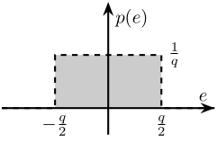
The variance (or time-average power) of the quantization noise is expressed by eqref:eq:detail_instrumentation_quant_power.
\begin{equation}\label{eq:detail_instrumentation_quant_power} P_q = ∫-q/2q/2 e^2 p(e) de = \frac{q^2}{12}
\end{equation}
To compute the power spectral density of the quantization noise, which is defined as the Fourier transform of the noise's autocorrelation function, it is assumed that noise samples are uncorrelated. Under this assumption, the autocorrelation function approximates a delta function in the time domain. Since the Fourier transform of a delta function equals one, the power spectral density becomes frequency-independent (white noise).
By Parseval's theorem, the power spectral density of the quantization noise $\Phi_q$ can be linked to the ADC sampling frequency and quantization step size eqref:eq:detail_instrumentation_psd_quant_noise.
\begin{equation}\label{eq:detail_instrumentation_psd_quant_noise} ∫-F_s/2F_s/2 Φ_q(f) d f = ∫-q/2q/2 e^2 p(e) de \quad \Longrightarrow \quad Φ_q = \frac{q^2}{12 F_s} = \frac{≤ft(\frac{Δ V}{2^n}\right)^2}{12 F_s} \quad \text{in } ≤ft[ \frac{V^2}{\text{Hz}} \right]
\end{equation}
From a specified noise amplitude spectral density $\Gamma_{\text{max}}$, the minimum number of bits required to keep quantization noise below $\Gamma_{\text{max}}$ is calculated using eqref:eq:detail_instrumentation_min_n.
\begin{equation}\label{eq:detail_instrumentation_min_n} n = \text{log}_2 ≤ft( \frac{Δ V}{\sqrt{12 F_s} ⋅ Γ_{\text{max}}} \right)
\end{equation}
With a sampling frequency $F_s = 10\,\text{kHz}$, an input range $\Delta V = 20\,V$ and a maximum allowed ASD $\Gamma_{\text{max}} = 11\,\mu V/\sqrt{Hz}$, the minimum number of bits is $n_{\text{min}} = 12.4$, which is readily achievable with commercial ADCs.
delta_V = 20; % +/-10 V
Fs = 10e3; % Sampling Frequency [Hz]
max_adc_asd = 11e-6; % V/sqrt(Hz)

min_n = log2(delta_V/(sqrt(12*Fs)*max_adc_asd))
%% Estimate quantization noise of the ADC
delta_V = 20; % +/-10 V
n = 16; % number of bits
Fs = 10e3; % [Hz]
q = delta_V/2^n; % Quantization in [V]
q_psd = q^2/12/Fs; % Quantization noise Power Spectral Density [V^2/Hz]
q_asd = sqrt(q_psd) % Quantization noise Amplitude Spectral Density [V/sqrt(Hz)]DAC Output voltage noise
Similar to the ADC requirements, the DAC output voltage noise ASD should not exceed $14\,\mu V/\sqrt{\text{Hz}}$. This specification corresponds to a $\pm 10\,V$ DAC with 13-bit resolution, which is easily attainable with current technology.
Choice of the ADC and DAC Board
Based on the preceding analysis, the selection of suitable ADC and DAC components is straightforward.
For optimal synchronicity, a Speedgoat-integrated solution was chosen. The selected model is the IO131, which features 16 analog inputs based on the AD7609 with 16-bit resolution, $\pm 10\,V$ range, maximum sampling rate of 200kSPS, simultaneous sampling, and differential inputs allowing the use of shielded twisted pairs for enhanced noise immunity. The board also includes 8 analog outputs based on the AD5754R with 16-bit resolution, $\pm 10\,V$ range, conversion time of $10\,\mu s$, and simultaneous update capability.
Although noise specifications are not explicitly provided in the datasheet, the 16-bit resolution should ensure performance well below the established requirements. This will be experimentally verified in Section ref:sec:detail_instrumentation_characterization.
Relative Displacement Sensors
The specifications for the relative displacement sensors include sufficient compactness for integration within each strut, noise levels below $6\,\text{nm RMS}$ (derived from the $15\,\text{nm RMS}$ vertical error requirement for the system divided by the contributions of six struts), and a measurement range exceeding $100\,\mu m$.
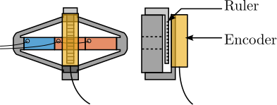
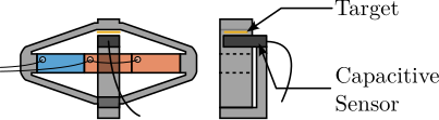
Several sensor technologies are capable of meeting these requirements cite:&fleming13_review_nanom_resol_posit_sensor. These include optical encoders (Figure ref:fig:detail_instrumentation_sensor_encoder), capacitive sensors (Figure ref:fig:detail_instrumentation_sensor_capacitive), and eddy current sensors (Figure ref:fig:detail_instrumentation_sensor_eddy_current), each with their own advantages and implementation considerations.
From an implementation perspective, capacitive and eddy current sensors offer a slight advantage as they can be quite compact and can measure in line with the APA, as illustrated in Figure ref:fig:detail_instrumentation_capacitive_implementation. In contrast, optical encoders are bigger and they must be offset from the strut's action line, which introduces potential measurement errors (Abbe errors) due to potential relative rotations between the two ends of the APA, as shown in Figure ref:fig:detail_instrumentation_encoder_implementation.
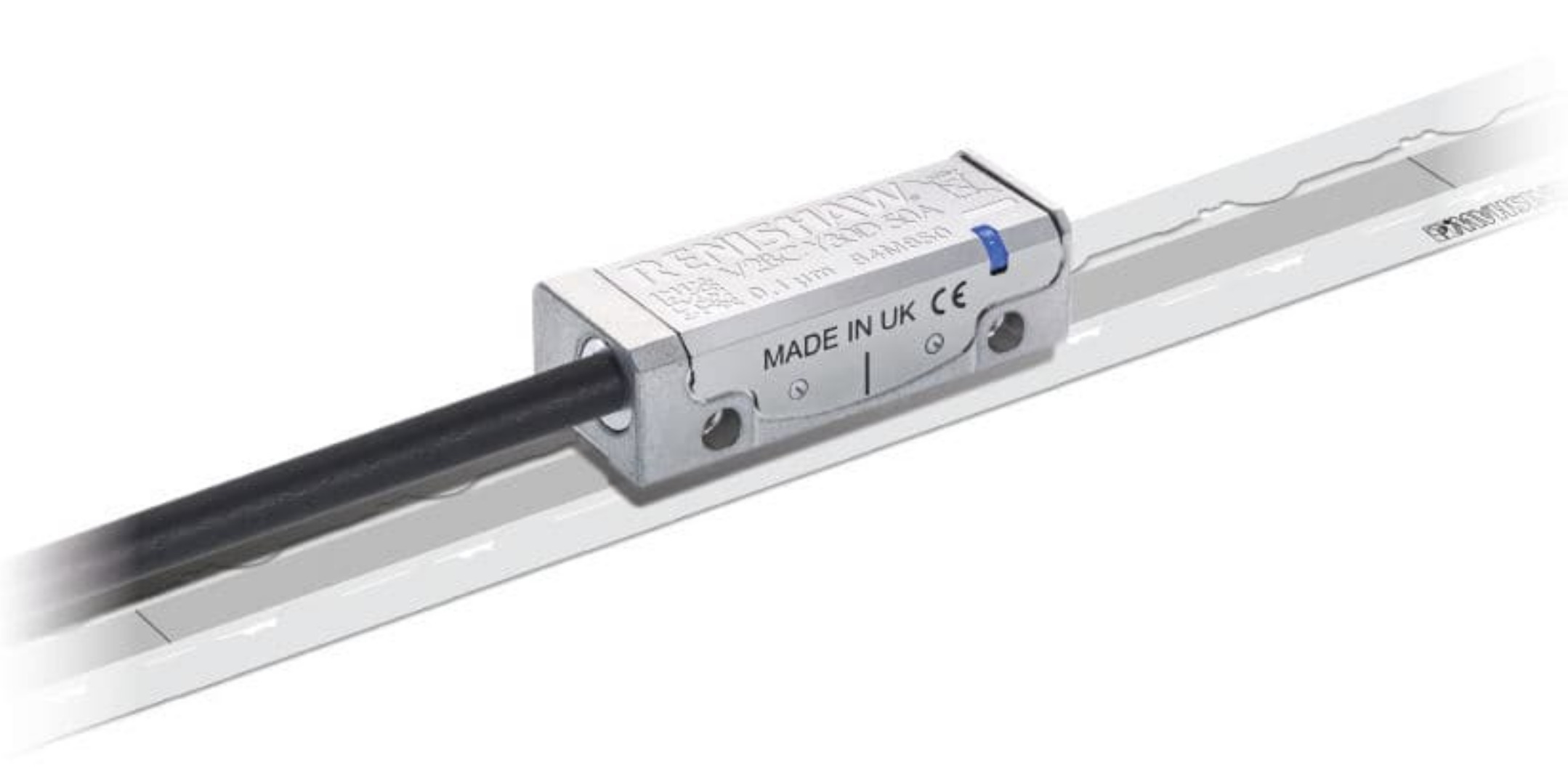
A significant consideration in the sensor selection process was the fact that sensor signals must pass through an electrical slip-ring due to the continuous spindle rotation. Measurements conducted on the slip-ring integrated in the micro-station revealed substantial cross-talk between different slip-ring channels. To mitigate this issue, preference was given to sensors that transmit displacement measurements digitally, as these are inherently less susceptible to noise and cross-talk. Based on this criterion, an optical encoder with digital output was selected, where signal interpolation is performed directly in the sensor head.
The specifications of the considered relative motion sensor, the Renishaw Vionic, are summarized in Table ref:tab:detail_instrumentation_sensor_specs, alongside alternative options that were considered.
| Specification | Renishaw Vionic | LION CPL190 | Cedrat ECP500 |
|---|---|---|---|
| Technology | Digital Encoder | Capacitive | Eddy Current |
| Bandwidth $> 5\,\text{kHz}$ | $> 500\,\text{kHz}$ | 10kHz | 20kHz |
| Noise $< 6\,nm\,\text{RMS}$ | 1.6 nm rms | 4 nm rms | 15 nm rms |
| Range $> 100\,\mu m$ | Ruler length | 250 um | 500um |
| In line measurement | $\times$ | $\times$ | |
| Digital Output | $\times$ |
Characterization of Instrumentation
<<sec:detail_instrumentation_characterization>>
Introduction ignore
Following the procurement of all instrumentation components, individual testing was conducted to verify their compliance with the specified requirements.
Analog to Digital Converters
Measured Noise
The measurement of ADC noise was performed by short-circuiting its input with a $50\,\Omega$ resistor and recording the digital values at a sampling rate of $10\,\text{kHz}$. The amplitude spectral density of the recorded values was computed and is presented in Figure ref:fig:detail_instrumentation_adc_noise_measured. The ADC noise exhibits characteristics of white noise with an amplitude spectral density of $5.6\,\mu V/\sqrt{\text{Hz}}$ (equivalent to $0.4\,\text{mV RMS}$), which satisfies the established specifications. All ADC channels demonstrated similar performance, so only one channel's noise profile is shown.
If necessary, oversampling can be applied to further reduce the noise cite:lab13_improv_adc. To gain $w$ additional bits of resolution, the oversampling frequency $f_{os}$ should be set to $f_{os} = 4^w \cdot F_s$. Given that the ADC can operate at 200kSPS while the real-time controller runs at 10kSPS, an oversampling factor of 16 can be employed to gain approximately two additional bits of resolution (reducing noise by a factor of 4). This approach is effective because the noise approximates white noise and its amplitude exceeds 1 LSB (0.3 mV) cite:hauser91_princ_overs_conver.
%% ADC noise
adc = load("2023-08-23_15-42_io131_adc_noise.mat");

% Spectral Analysis parameters
Ts = 1e-4;
Nfft = floor(1/Ts);
win = hanning(Nfft);
Noverlap = floor(Nfft/2);
% Identification of the transfer function from Va to di
[pxx, f] = pwelch(detrend(adc.adc_1, 0), win, Noverlap, Nfft, 1/Ts);

adc.pxx = pxx;
adc.f = f;

% estimated mean ASD
sprintf('Mean ASD of the ADC: %.1f uV/sqrt(Hz)', 1e6*sqrt(mean(adc.pxx)))
sprintf('Specifications: %.1f uV/sqrt(Hz)', 1e6*max_adc_asd)

% estimated RMS
sprintf('RMS of the ADC: %.2f mV RMS', 1e3*rms(detrend(adc.adc_1,0)))
sprintf('RMS specifications: %.2f mV RMS', max_adc_rms)

% Estimate quantization noise of the IO318 ADC
delta_V = 20; % +/-10 V
n = 16; % number of bits
Fs = 10e3; % [Hz]

adc.q = delta_V/2^n; % Quantization in [V]
adc.q_psd = adc.q^2/12/Fs; % Quantization noise Power Spectral Density [V^2/Hz]
adc.q_asd = sqrt(adc.q_psd); % Quantization noise Amplitude Spectral Density [V/sqrt(Hz)]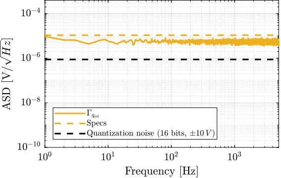
Reading of piezoelectric force sensor
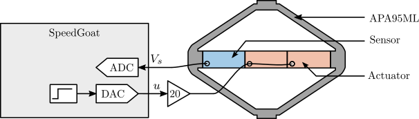
To further validate the ADC's capability to effectively measure voltage generated by a piezoelectric stack, a test was conducted using the APA95ML. The setup is illustrated in Figure ref:fig:detail_instrumentation_force_sensor_adc_setup, where two stacks are used as actuators (connected in parallel) and one stack serves as a sensor. The voltage amplifier employed in this setup has a gain of 20.
Step signals with an amplitude of $1\,V$ were generated using the DAC, and the ADC signal was recorded. The excitation signal (steps) and the measured voltage across the sensor stack are displayed in Figure ref:fig:detail_instrumentation_step_response_force_sensor.
Two notable observations were made: an offset voltage of $2.26\,V$ was present, and the measured voltage exhibited an exponential decay response to the step input. These phenomena can be explained by examining the electrical schematic shown in Figure ref:fig:detail_instrumentation_force_sensor_adc, where the ADC has an input impedance $R_i$ and an input bias current $i_n$.
The input impedance $R_i$ of the ADC, in combination with the capacitance $C_p$ of the piezoelectric stack sensor, forms an RC circuit with a time constant $\tau = R_i C_p$. The charge generated by the piezoelectric effect across the stack's capacitance gradually discharges into the input resistor of the ADC. Consequently, the transfer function from the generated voltage $V_p$ to the measured voltage $V_{\text{ADC}}$ is a first-order high-pass filter with the time constant $\tau$.
An exponential curve was fitted to the experimental data, yielding a time constant $\tau = 6.5\,s$. With the capacitance of the piezoelectric sensor stack being $C_p = 4.4\,\mu F$, the internal impedance of the Speedgoat ADC was calculated as $R_i = \tau/C_p = 1.5\,M\Omega$, which closely aligns with the specified value of $1\,M\Omega$ found in the datasheet.
%% Read force sensor voltage with the ADC
load('force_sensor_steps.mat', 't', 'encoder', 'u', 'v');

% Exponential fit to compute the time constant
% Fit function
f_exp = @(b,x) b(1).*exp(-b(2).*x) + b(3);

% Three steps are performed at the following time intervals:
t_s = [ 2.5, 23;
       23.8, 35;
       35.8, 50];

tau = zeros(size(t_s, 1),1); % Time constant [s]
V0  = zeros(size(t_s, 1),1); % Offset voltage [V]
a   = zeros(size(t_s, 1),1); %

for t_i = 1:size(t_s, 1)
    t_cur = t(t_s(t_i, 1) < t & t < t_s(t_i, 2));
    t_cur = t_cur - t_cur(1);
    y_cur = v(t_s(t_i, 1) < t & t < t_s(t_i, 2));

    nrmrsd = @(b) norm(y_cur - f_exp(b,t_cur)); % Residual Norm Cost Function
    B0 = [0.5, 0.15, 2.2];                        % Choose Appropriate Initial Estimates
    [B,rnrm] = fminsearch(nrmrsd, B0);     % Estimate Parameters ‘B’

    a(t_i)   = B(1);
    tau(t_i) = 1/B(2);
    V0(t_i)  = B(3);
end

% Data to show the exponential fit
t_fit_1 = linspace(t_s(1,1), t_s(1,2), 100);
y_fit_1 = f_exp([a(1),1/tau(1),V0(1)], t_fit_1-t_s(1,1));

t_fit_2 = linspace(t_s(2,1), t_s(2,2), 100);
y_fit_2 = f_exp([a(2),1/tau(2),V0(2)], t_fit_2-t_s(2,1));

t_fit_3 = linspace(t_s(3,1), t_s(3,2), 100);
y_fit_3 = f_exp([a(3),1/tau(3),V0(3)], t_fit_3-t_s(3,1));

% Speedgoat ADC input impedance
Cp = 4.4e-6; % [F]
Rin = abs(mean(tau))/Cp; % [Ohm]

% Estimated input bias current
in = mean(V0)/Rin; % [A]

% Resistor added in parallel to the force sensor
fc = 0.5; % Wanted corner frequency [Hz]
Ra = Rin/(2*pi*fc*Cp*Rin - 1); % [Ohm]

% New ADC offset voltage
V_offset = Ra*Rin/(Ra + Rin) * in; % [V]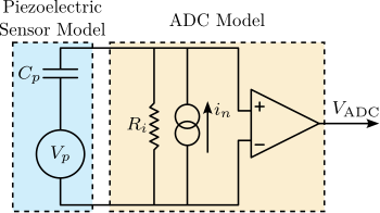
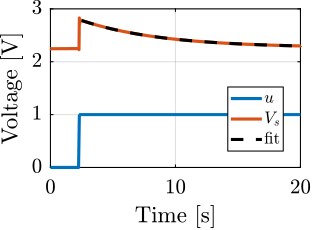
The constant voltage offset can be explained by the input bias current $i_n$ of the ADC, represented in Figure ref:fig:detail_instrumentation_force_sensor_adc. At DC, the impedance of the piezoelectric stack is much larger than the input impedance of the ADC, and therefore the input bias current $i_n$ passing through the internal resistance $R_i$ produces a constant voltage offset $V_{\text{off}} = R_i \cdot i_n$. The input bias current $i_n$ is estimated from $i_n = V_{\text{off}}/R_i = 1.5\mu A$.
In order to reduce the input voltage offset and to increase the corner frequency of the high pass filter, a resistor $R_p$ can be added in parallel to the force sensor, as illustrated in Figure ref:fig:detail_instrumentation_force_sensor_adc_R. This modification produces two beneficial effects: a reduction of input voltage offset through the relationship $V_{\text{off}} = (R_p R_i)/(R_p + R_i) i_n$, and an increase in the high pass corner frequency $f_c$ according to the equations $\tau = 1/(2\pi f_c) = (R_i R_p)/(R_i + R_p) C_p$.
To validate this approach, a resistor $R_p \approx 82\,k\Omega$ was added in parallel with the force sensor as shown in Figure ref:fig:detail_instrumentation_force_sensor_adc_R. After incorporating this resistor, the same step response tests were performed, with results displayed in Figure ref:fig:detail_instrumentation_step_response_force_sensor_R. The measurements confirmed the expected improvements, with a substantially reduced offset voltage ($V_{\text{off}} = 0.15\,V$) and a much faster time constant ($\tau = 0.45\,s$). These results validate both the model of the ADC and the effectiveness of the added parallel resistor as a solution.
%% Read force sensor voltage with the ADC with added 82.7kOhm resistor
load('force_sensor_steps_R_82k7.mat', 't', 'encoder', 'u', 'v');

% Step times
t_s = [1.9,  6;
       8.5, 13;
      15.5, 21;
      22.6, 26;
      30.0, 36;
      37.5, 41;
      46.2, 49.5]; % [s]

tau = zeros(size(t_s, 1),1); % Time constant [s]
V0  = zeros(size(t_s, 1),1); % Offset voltage [V]
a   = zeros(size(t_s, 1),1); %

for t_i = 1:size(t_s, 1)
    t_cur = t(t_s(t_i, 1) < t & t < t_s(t_i, 2));
    t_cur = t_cur - t_cur(1);
    y_cur = v(t_s(t_i, 1) < t & t < t_s(t_i, 2));

    nrmrsd = @(b) norm(y_cur - f_exp(b,t_cur)); % Residual Norm Cost Function
    B0 = [0.5, 0.1, 2.2];                        % Choose Appropriate Initial Estimates
    [B,rnrm] = fminsearch(nrmrsd, B0);     % Estimate Parameters ‘B’

    a(t_i)   = B(1);
    tau(t_i) = 1/B(2);
    V0(t_i)  = B(3);
end

% Data to show the exponential fit
t_fit_1 = linspace(t_s(1,1), t_s(1,2), 100);
y_fit_1 = f_exp([a(1),1/tau(1),V0(1)], t_fit_1-t_s(1,1));

t_fit_2 = linspace(t_s(2,1), t_s(2,2), 100);
y_fit_2 = f_exp([a(2),1/tau(2),V0(2)], t_fit_2-t_s(2,1));

t_fit_3 = linspace(t_s(3,1), t_s(3,2), 100);
y_fit_3 = f_exp([a(3),1/tau(3),V0(3)], t_fit_3-t_s(3,1));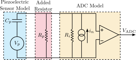

Instrumentation Amplifier
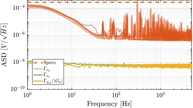
Because the ADC noise may be too low to measure the noise of other instruments (anything below $5.6\,\mu V/\sqrt{\text{Hz}}$ cannot be distinguished from the noise of the ADC itself), a low noise instrumentation amplifier was employed. A Femto DLPVA-101-B-S amplifier with adjustable gains from 20dB up to 80dB was selected for this purpose.
The first step was to characterize the input2 noise of the amplifier. This was accomplished by short-circuiting its input with a $50\,\Omega$ resistor and measuring the output voltage with the ADC (Figure ref:fig:detail_instrumentation_femto_meas_setup). The maximum amplifier gain of 80dB (equivalent to 10000) was utilized for this measurement.
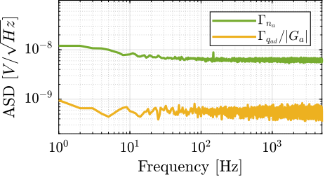
The measured voltage $n$ was then divided by 10000 to determine the equivalent noise at the input of the voltage amplifier $n_a$. In this configuration, the noise contribution from the ADC $q_{ad}$ is rendered negligible due to the high gain employed. The resulting amplifier noise amplitude spectral density $\Gamma_{n_a}$ and the (negligible) contribution of the ADC noise are presented in Figure ref:fig:detail_instrumentation_femto_input_noise.
\begin{tikzpicture}
  \node[block={0.6cm}{0.6cm}] (const) {$0$};
  % Pre Amp
  \node[addb, right=0.4 of const] (addna) {};
  \node[block, right=0.3 of addna] (Ga) {$G_a(s)$};

  % ADC
  \node[addb, right=0.8 of Ga] (addqad){};
  \node[ADC, right=0.3 of addqad] (ADC) {ADC};

  \draw[->] (const.east) -- (addna.west);
  \draw[->] (addna.east) -- (Ga.west);
  \draw[->] (Ga.east)    -- (addqad.west);
  \draw[->] (addqad.east) -- (ADC.west);
  \draw[->] (ADC.east)    -- node[sloped]{$/$} ++(0.8, 0) node[above left]{$n$};

  \draw[<-] (addna.north)  -- ++(0, 0.6) node[below right](na){$n_{a}$};
  \draw[<-] (addqad.north) -- ++(0, 0.6) node[below right](qad){$q_{ad}$};

  \coordinate[] (top) at (na.north);
  \coordinate[] (bot) at (Ga.south);

  % 5113
  \begin{scope}[on background layer]
    \node[fit={(addna.west|-bot) (Ga.east|-top)}, inner sep=4pt, draw, dashed, fill=colorgreen!20!white] (P) {};
    \node[above] at (P.north) {Pre Amp};
  \end{scope}

  % ADC
  \begin{scope}[on background layer]
    \node[fit={(addqad.west|-bot) (ADC.east|-top)}, inner sep=4pt, draw, dashed, fill=coloryellow!20!white] (P) {};
    \node[above] at (P.north) {ADC};
  \end{scope}
\end{tikzpicture}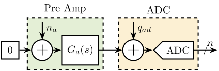
\hfill
Digital to Analog Converters
Output Voltage Noise
To measure the output noise of the DAC, the setup schematically represented in Figure ref:fig:detail_instrumentation_dac_setup was utilized. The DAC was configured to output a constant voltage (zero in this case), and the gain of the pre-amplifier was adjusted such that the measured amplified noise was significantly larger than the noise of the ADC.
The Amplitude Spectral Density $\Gamma_{n_{da}}(\omega)$ of the measured signal was computed, and verification was performed to confirm that the contributions of ADC noise and amplifier noise were negligible in the measurement.
The resulting Amplitude Spectral Density of the DAC's output voltage is displayed in Figure ref:fig:detail_instrumentation_dac_output_noise. The noise profile is predominantly white with an ASD of $0.6\,\mu V/\sqrt{\text{Hz}}$. Minor $50\,\text{Hz}$ noise is present, along with some low frequency $1/f$ noise, but these are not expected to pose issues as they are well within specifications. It should be noted that all DAC channels demonstrated similar performance, so only one channel measurement is presented.
\begin{tikzpicture}
  \node[block={0.6cm}{0.6cm}] (const) {$0$};

  % DAC
  \node[DAC, right=0.4 of const] (DAC) {DAC};
  \node[addb, right=0.3 of DAC] (addnda){};

  % Pre Amp
  \node[addb, right=0.8 of addnda] (addna) {};
  \node[block, right=0.3 of addna] (Ga) {$G_a(s)$};

  % ADC
  \node[addb, right=0.8 of Ga] (addqad){};
  \node[ADC, right=0.3 of addqad] (ADC) {ADC};

  \draw[->] (const.east) -- node[sloped]{$/$} (DAC.west);
  \draw[->] (DAC.east) -- (addnda.west);
  \draw[->] (addnda.east) -- (addna.west);
  \draw[->] (addna.east) -- (Ga.west);
  \draw[->] (Ga.east) -- (addqad.west);
  \draw[->] (addqad.east) -- (ADC.west);
  \draw[->] (ADC.east) -- node[sloped]{$/$} ++(0.8, 0);

  \draw[<-] (addnda.north) -- ++(0, 0.6) node[below left](nda){$n_{da}$};
  \draw[<-] (addna.north)  -- ++(0, 0.6) node[below right](na){$n_{a}$};
  \draw[<-] (addqad.north) -- ++(0, 0.6) node[below right](qad){$q_{ad}$};

  \coordinate[] (top) at (na.north);
  \coordinate[] (bot) at (Ga.south);

  % DAC
  \begin{scope}[on background layer]
    \node[fit={(DAC.west|-bot) (addnda.east|-top)}, inner sep=4pt, draw, dashed, fill=colorblue!20!white] (P) {};
    \node[above] at (P.north) {DAC};
  \end{scope}

  % 5113
  \begin{scope}[on background layer]
    \node[fit={(addna.west|-bot) (Ga.east|-top)}, inner sep=4pt, draw, dashed, fill=colorgreen!20!white] (P) {};
    \node[above] at (P.north) {Pre Amp};
  \end{scope}

  % ADC
  \begin{scope}[on background layer]
    \node[fit={(addqad.west|-bot) (ADC.east|-top)}, inner sep=4pt, draw, dashed, fill=coloryellow!20!white] (P) {};
    \node[above] at (P.north) {ADC};
  \end{scope}
\end{tikzpicture}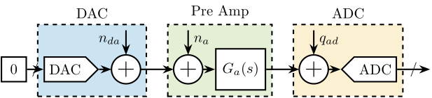
Delay from ADC to DAC
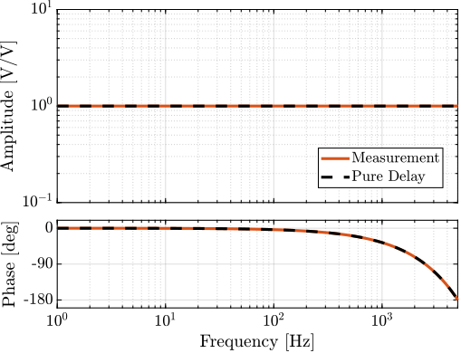
To measure the transfer function from DAC to ADC and verify that the bandwidth and latency of both instruments is sufficient, a direct connection was established between the DAC output and the ADC input. A white noise signal was generated by the DAC, and the ADC response was recorded.
The resulting frequency response function from the digital DAC signal to the digital ADC signal is presented in Figure ref:fig:detail_instrumentation_dac_adc_tf. The observed frequency response function corresponds to exactly one sample delay, which aligns with the specifications provided by the manufacturer.
%% Measure transfer function from DAC to ADC
data_dac_adc = load("2023-08-22_15-52_io131_dac_to_adc.mat");

% Frequency analysis parameters
Ts = 1e-4; % Sampling Time [s]
Nfft = floor(1.0/Ts);
win = hanning(Nfft);
Noverlap = floor(Nfft/2);

[G_dac_adc, f] = tfestimate(data_dac_adc.dac_1, data_dac_adc.adc_1, win, Noverlap, Nfft, 1/Ts);

%
G_delay = exp(-Ts*s);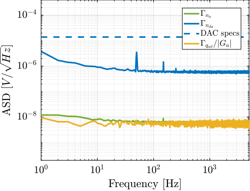
Piezoelectric Voltage Amplifier
Output Voltage Noise
The measurement setup for evaluating the PD200 amplifier noise is illustrated in Figure ref:fig:detail_instrumentation_pd200_setup. The input of the PD200 amplifier was shunted with a $50\,\Ohm$ resistor to ensure that only the inherent noise of the amplifier itself was measured. The pre-amplifier gain was increased to produce a signal substantially larger than the noise floor of the ADC. Two piezoelectric stacks from the APA95ML were connected to the PD200 output to provide an appropriate load for the amplifier.
\begin{tikzpicture}
  \node[block={0.6cm}{0.6cm}] (const) {$0$};

  % PD200
  \node[block, right=0.4 of const] (Gp){$G_p(s)$};
  \node[addb, right=0.3 of Gp] (addnp){};

  % Pre Amp
  \node[addb, right=0.8 of addnp] (addna) {};
  \node[block, right=0.3 of addna] (Ga) {$G_a(s)$};

  % ADC
  \node[addb, right=0.8 of Ga] (addqad){};
  \node[ADC, right=0.3 of addqad] (ADC) {ADC};

  \draw[->] (const.east) -- (Gp.west);
  \draw[->] (Gp.east) -- (addnp.west);
  \draw[->] (addnp.east) -- (addna.west);
  \draw[->] (addna.east) -- (Ga.west);
  \draw[->] (Ga.east) -- (addqad.west);
  \draw[->] (addqad.east) -- (ADC.west);
  \draw[->] (ADC.east) -- node[sloped]{$/$} ++(0.8, 0) node[above left]{$n$};

  \draw[<-] (addnp.north) -- ++(0, 0.6) node[below left](np){$n_{p}$};
  \draw[<-] (addna.north) -- ++(0, 0.6) node[below right](na){$n_{a}$};
  \draw[<-] (addqad.north) -- ++(0, 0.6) node[below right](qad){$q_{ad}$};

  \coordinate[] (top) at (na.north);
  \coordinate[] (bot) at (Ga.south);

  % PD200
  \begin{scope}[on background layer]
    \node[fit={(addnp.east|-bot) (Gp.west|-top)}, inner sep=4pt, draw, dashed, fill=colorred!20!white] (P) {};
    \node[above] at (P.north) {PD200};
  \end{scope}

  % 5113
  \begin{scope}[on background layer]
    \node[fit={(addna.west|-bot) (Ga.east|-top)}, inner sep=4pt, draw, dashed, fill=colorgreen!20!white] (P) {};
    \node[above] at (P.north) {Pre Amp};
  \end{scope}

  % ADC
  \begin{scope}[on background layer]
    \node[fit={(addqad.west|-bot) (ADC.east|-top)}, inner sep=4pt, draw, dashed, fill=coloryellow!20!white] (P) {};
    \node[above] at (P.north) {ADC};
  \end{scope}
\end{tikzpicture}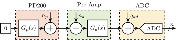
The Amplitude Spectral Density $\Gamma_{n}(\omega)$ of the signal measured by the ADC was computed. From this, the Amplitude Spectral Density of the output voltage noise of the PD200 amplifier $n_p$ was derived, accounting for the gain of the pre-amplifier according to eqref:eq:detail_instrumentation_amp_asd.
\begin{equation}\label{eq:detail_instrumentation_amp_asd} Γn_p(ω) = \frac{Γ_n(ω)}{|G_p(jω) G_a(jω)|}
\end{equation}
The computed Amplitude Spectral Density of the PD200 output noise is presented in Figure ref:fig:detail_instrumentation_pd200_noise. Verification was performed to confirm that the measured noise was predominantly from the PD200, with negligible contributions from the pre-amplifier noise or ADC noise. The measurements from all six amplifiers are displayed in this figure.
The noise spectrum of the PD200 amplifiers exhibits several sharp peaks. While the exact cause of these peaks is not fully understood, their amplitudes remain below the specified limits and should not adversely affect system performance.
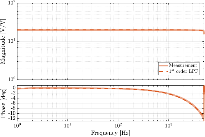
Small Signal Bandwidth
The small signal dynamics of all six PD200 amplifiers were characterized through frequency response measurements.
A logarithmic sweep sine excitation voltage was generated using the Speedgoat DAC with an amplitude of $0.1\,V$, spanning frequencies from $1\,\text{Hz}$ to $5\,\text{kHz}$. The output voltage of the PD200 amplifier was measured via the monitor voltage output of the amplifier, while the input voltage (generated by the DAC) was measured with a separate ADC channel of the Speedgoat system. This measurement approach eliminates the influence of ADC-DAC-related time delays in the results.
All six amplifiers demonstrated consistent transfer function characteristics. The amplitude response remains constant across a wide frequency range, and the phase shift is limited to less than 1 degree up to 500Hz, well within the specified requirements.
The identified dynamics shown in Figure ref:fig:detail_instrumentation_pd200_tf can be accurately modeled as either a first-order low-pass filter or as a simple constant gain.
Linear Encoders
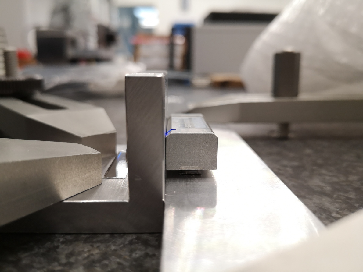
To measure the noise of the encoder, the head and ruler were rigidly fixed together to ensure that no actual motion would be detected. Under these conditions, any measured signal would correspond solely to the encoder noise.
The measurement setup is shown in Figure ref:fig:detail_instrumentation_vionic_bench. To minimize environmental disturbances, the entire bench was covered with a plastic bubble sheet during measurements.
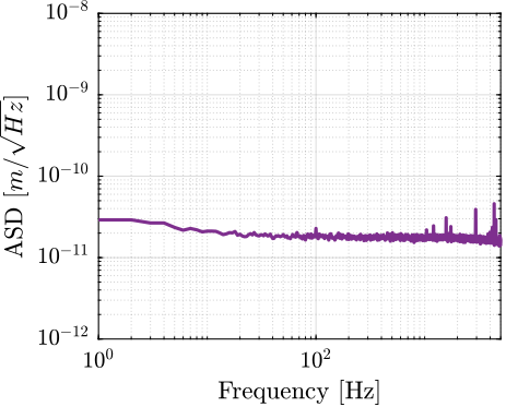
The amplitude spectral density of the measured displacement (which represents the measurement noise) is presented in Figure ref:fig:detail_instrumentation_vionic_asd. The noise profile exhibits characteristics of white noise with an amplitude of approximately $1\,\text{nm RMS}$, which complies with the system requirements.
\hfill
Noise budgeting from measured instrumentation noise
After characterizing all instrumentation components individually, their combined effect on the sample's vibration was assessed using the multi-body model developed earlier.
The vertical motion induced by the noise sources, specifically the ADC noise, DAC noise, and voltage amplifier noise, is presented in Figure ref:fig:detail_instrumentation_cl_noise_budget.
The total motion induced by all noise sources combined is approximately $1.5\,\text{nm RMS}$, which remains well within the specified limit of $15\,\text{nm RMS}$. This confirms that the selected instrumentation, with its measured noise characteristics, is suitable for the intended application.
%% Estimate the resulting errors induced by noise of instruments
f = dac.f;

% Vertical direction
psd_z_dac = 6*(abs(squeeze(freqresp(Gd('z', 'nda1' ), f, 'Hz'))).^2).*dac.pxx;
psd_z_adc = 6*(abs(squeeze(freqresp(Gd('z', 'nad1' ), f, 'Hz'))).^2).*adc.pxx;
psd_z_amp = 6*(abs(squeeze(freqresp(Gd('z', 'namp1'), f, 'Hz'))).^2).*pd200{1}.pxx;
psd_z_enc = 6*(abs(squeeze(freqresp(Gd('z', 'ddL1' ), f, 'Hz'))).^2).*enc{1}.pxx;
psd_z_tot = psd_z_dac + psd_z_adc + psd_z_amp + psd_z_enc;

rms_z_dac = sqrt(trapz(f, psd_z_dac));
rms_z_adc = sqrt(trapz(f, psd_z_adc));
rms_z_amp = sqrt(trapz(f, psd_z_amp));
rms_z_enc = sqrt(trapz(f, psd_z_enc));
rms_z_tot = sqrt(trapz(f, psd_z_tot));

% Lateral direction
psd_y_dac = 6*(abs(squeeze(freqresp(Gd('y', 'nda1' ), f, 'Hz'))).^2).*dac.pxx;
psd_y_adc = 6*(abs(squeeze(freqresp(Gd('y', 'nad1' ), f, 'Hz'))).^2).*adc.pxx;
psd_y_amp = 6*(abs(squeeze(freqresp(Gd('y', 'namp1'), f, 'Hz'))).^2).*pd200{1}.pxx;
psd_y_enc = 6*(abs(squeeze(freqresp(Gd('y', 'ddL1' ), f, 'Hz'))).^2).*enc{1}.pxx;
psd_y_tot = psd_y_dac + psd_y_adc + psd_y_amp + psd_y_enc;

rms_y_tot = sqrt(trapz(f, psd_y_tot));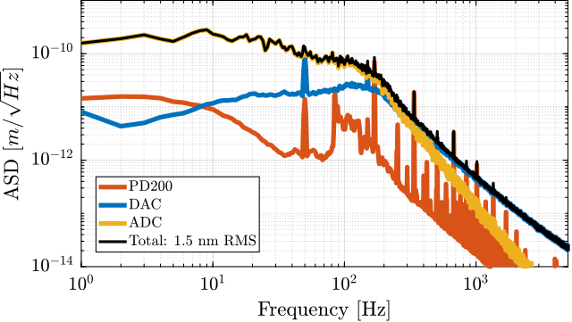
Conclusion
<<sec:detail_instrumentation_conclusion>>
This section has presented a comprehensive approach to the selection and characterization of instrumentation for the nano active stabilization system. The multi-body model developed earlier proved invaluable for incorporating instrumentation components and their associated noise sources into the system analysis. From the most stringent requirement (i.e. the specification on vertical sample motion limited to 15 nm RMS), detailed specifications for each noise source were methodically derived through dynamic error budgeting.
Based on these specifications, appropriate instrumentation components were selected for the system. The selection process revealed certain challenges, particularly with voltage amplifiers, where manufacturer datasheets often lacked crucial information needed for accurate noise budgeting, such as amplitude spectral densities under specific load conditions. Despite these challenges, suitable components were identified that theoretically met all requirements.
The selected instrumentation (including the IO131 ADC/DAC from Speedgoat, PD200 piezoelectric voltage amplifiers from PiezoDrive, and Vionic linear encoders from Renishaw) was procured and thoroughly characterized. Initial measurements of the ADC system revealed an issue with force sensor readout related to input bias current, which was successfully addressed by adding a parallel resistor to optimize the measurement circuit.
All components were found to meet or exceed their respective specifications. The ADC demonstrated noise levels of $5.6\,\mu V/\sqrt{\text{Hz}}$ (versus the $11\,\mu V/\sqrt{\text{Hz}}$ specification), the DAC showed $0.6\,\mu V/\sqrt{\text{Hz}}$ (versus $14\,\mu V/\sqrt{\text{Hz}}$ required), the voltage amplifiers exhibited noise well below the $280\,\mu V/\sqrt{\text{Hz}}$ limit, and the encoders achieved $1\,\text{nm RMS}$ noise (versus the $6\,\text{nm RMS}$ specification).
Finally, the measured noise characteristics of all instrumentation components were incorporated into the multi-body model to predict the actual system performance. The combined effect of all noise sources was estimated to induce vertical sample vibrations of only $1.5\,\text{nm RMS}$, which is substantially below the $15\,\text{nm RMS}$ requirement. This rigorous methodology spanning requirement formulation, component selection, and experimental characterization validates the instrumentation's ability to fulfill the nano active stabilization system's demanding performance specifications.