Voltage Amplifier PD200 - Test Bench
Table of Contents
The goal of this test bench is to characterize the Voltage amplifier PD200 from PiezoDrive.
The documentation of the PD200 is accessible here.

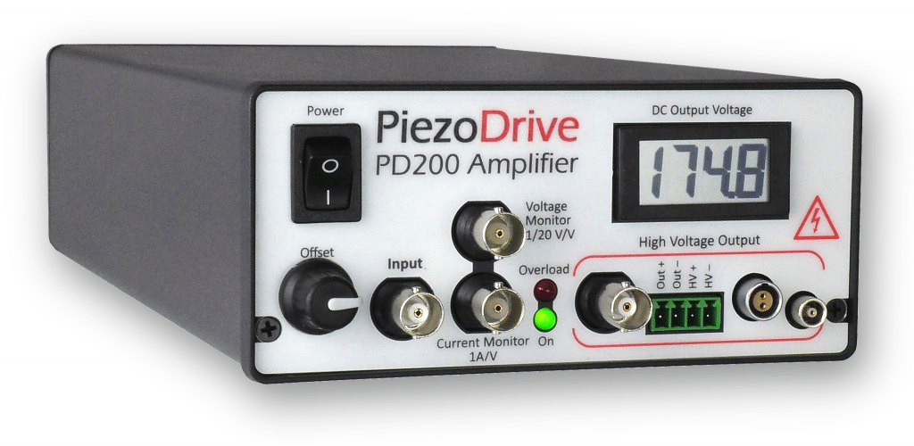
Figure 1: Picture of the PD200 Voltage Amplifier
1 Voltage Amplifier Requirements
| Specification | |
|---|---|
| Continuous Current | > 50 [mA] |
| Output Voltage Noise (1-200Hz) | < 2 [mV rms] |
| Voltage Input Range | +/- 10 [V] |
| Voltage Output Range | -20 [V] to 150 [V] |
| Small signal bandwidth (-3dB) | > 5 [kHz] |
2 PD200 Expected characteristics
| Characteristics | Manual | Specification |
|---|---|---|
| Input Voltage Range | +/- 10 [V] | +/- 10 [V] |
| Output Voltage Range | -50/150 [V] | -20/150 [V] |
| Gain | 20 [V/V] | |
| Maximum RMS current | 0.9 [A] | > 50 [mA] |
| Maximum Pulse current | 10 [A] | |
| Slew Rate | 150 [V/us] | |
| Noise (10uF load) | 0.7 [mV RMS] | < 2 [mV rms] |
| Small Signal Bandwidth (10uF load) | 7.4 [kHz] | > 5 [kHz] |
| Large Signal Bandwidth (150V, 10uF) | 300 [Hz] |
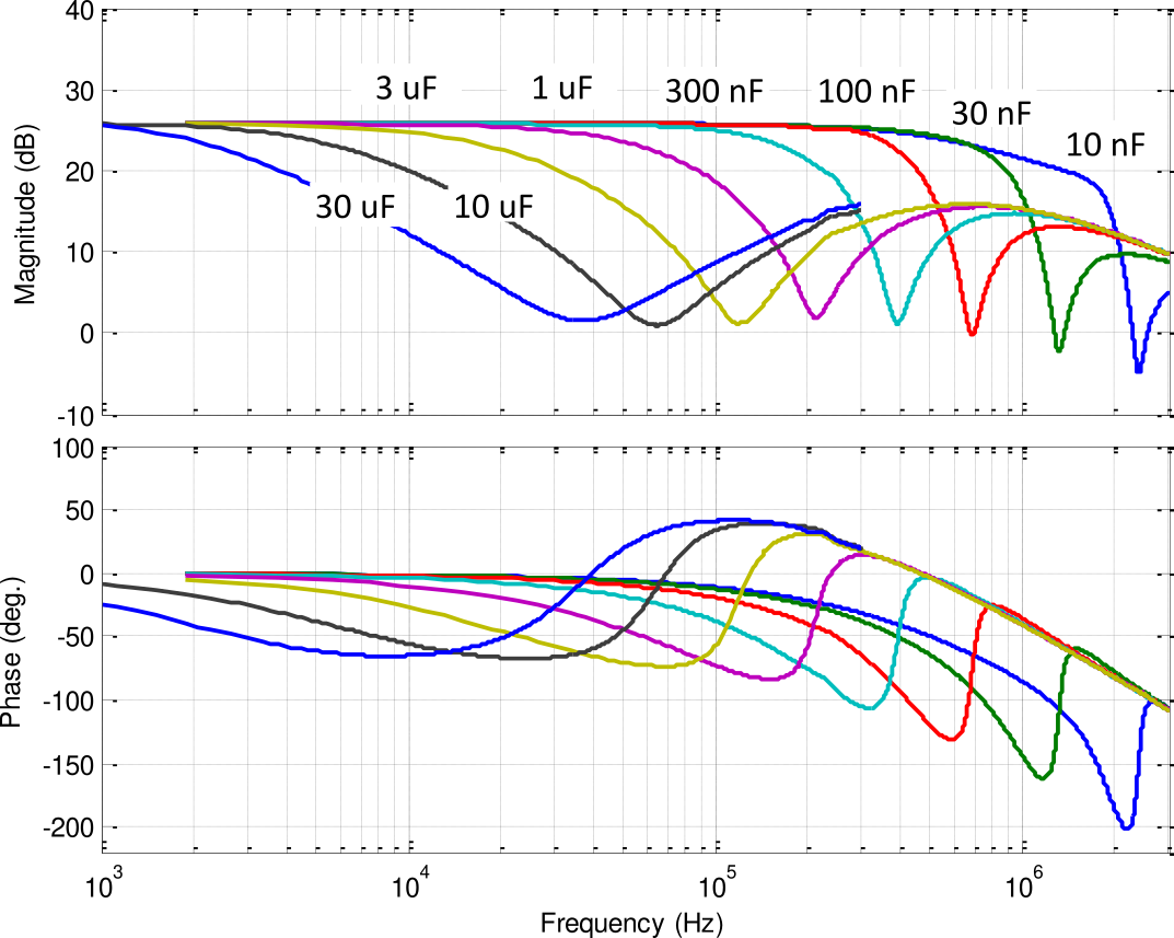
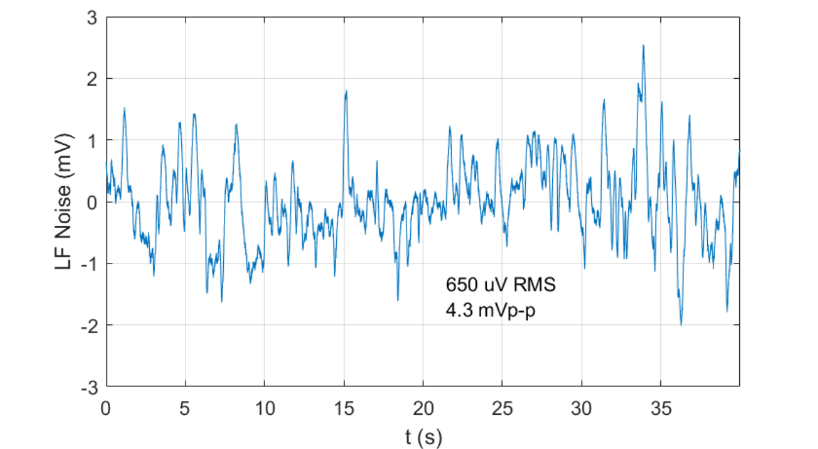
For a load capacitance of \(10\,\mu F\), the expected \(-3\,dB\) bandwidth is \(6.4\,kHz\) (Figure 2) and the low frequency noise is \(650\,\mu V\,\text{rms}\) (Figure 3).

Figure 2: Expected small signal bandwidth

Figure 3: Expected Low frequency noise from 0.03Hz to 20Hz
3 Voltage Amplifier Model
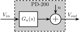
The Amplifier is characterized by its dynamics \(G_a(s)\) from voltage inputs \(V_{in}\) to voltage output \(V_{out}\). Ideally, the gain from \(V_{in}\) to \(V_{out}\) is constant over a wide frequency band with very small phase drop.
It is also characterized by its output noise \(n\). This noise is described by its Power Spectral Density.

Figure 4: Model of the voltage amplifier
4 Noise measurement
4.1 Setup
Here are the documentation of the equipment used for this test bench:
- Voltage Amplifier PD200
- Load Capacitor EPCOS 10μF Multilayer Ceramic Capacitor
- Low Noise Voltage Amplifier EG&G 5113
- Speedgoat ADC IO313
The output noise of the voltage amplifier PD200 is foreseen to be around 1mV rms in a bandwidth from DC to 1MHz. If we suppose a white noise, this correspond to an amplitude spectral density:
\begin{equation} \phi_{n} \approx \frac{1\,mV}{\sqrt{1\,MHz}} = 1 \frac{\mu V}{\sqrt{Hz}} \end{equation}The RMS noise begin very small compare to the ADC resolution, we must amplify the noise before digitizing the signal. The added noise of the instrumentation amplifier should be much smaller than the noise of the PD200. We use the amplifier EG&G 5113 that have a noise of \(\approx 4 nV/\sqrt{Hz}\) referred to its input which is much smaller than the noise induced by the PD200.
The gain of the low-noise amplifier can be increased until the full range of the ADC is used. This gain should be around 1000.

Figure 5: Schematic of the test bench to measure the Power Spectral Density of the Voltage amplifier noise \(n\)
4.2 Results
5 Transfer Function measurement
5.1 Setup
In order to measure the transfer function from the input voltage \(V_{in}\) to the output voltage \(V_{out}\), the test bench shown in Figure 6 is used.
Here are the documentation of the equipment used for this test bench:
- Voltage Amplifier PD200
- Load Capacitor EPCOS 10μF Multilayer Ceramic Capacitor
- Speedgoat DAC/ADC IO313
For this measurement, the sampling frequency of the Speedgoat ADC should be as high as possible.

Figure 6: Schematic of the test bench to estimate the dynamics from voltage input \(V_{in}\) to voltage output \(V_{out}\)
5.2 Results
6 Conclusion
| Characteristics | Measurement | Manual | Specification |
|---|---|---|---|
| Input Voltage Range | - | +/- 10 [V] | +/- 10 [V] |
| Output Voltage Range | - | -50/150 [V] | -20/150 [V] |
| Gain | 20 [V/V] | - | |
| Maximum RMS current | 0.9 [A] | > 50 [mA] | |
| Maximum Pulse current | 10 [A] | - | |
| Slew Rate | 150 [V/us] | - | |
| Noise (10uF load) | 0.7 [mV RMS] | < 2 [mV rms] | |
| Small Signal Bandwidth (10uF load) | 7.4 [kHz] | > 5 [kHz] | |
| Large Signal Bandwidth (150V, 10uF) | 300 [Hz] | - |